MT-002 TUTORIAL What the Nyquist Criterion Means to Your
advertisement
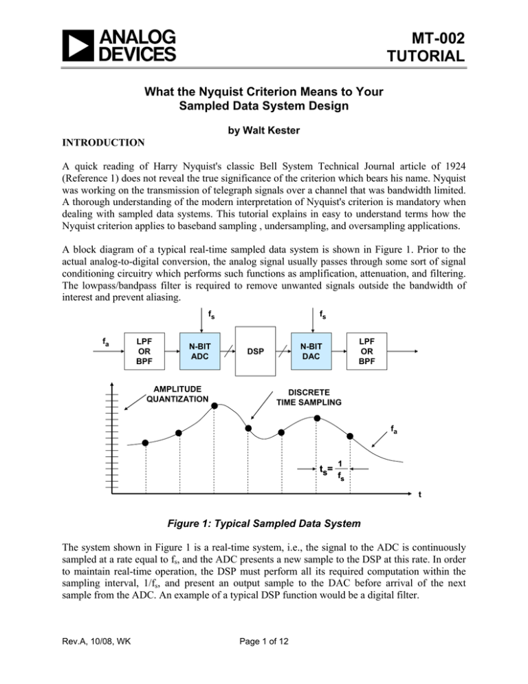
MT-002 TUTORIAL What the Nyquist Criterion Means to Your Sampled Data System Design by Walt Kester INTRODUCTION A quick reading of Harry Nyquist's classic Bell System Technical Journal article of 1924 (Reference 1) does not reveal the true significance of the criterion which bears his name. Nyquist was working on the transmission of telegraph signals over a channel that was bandwidth limited. A thorough understanding of the modern interpretation of Nyquist's criterion is mandatory when dealing with sampled data systems. This tutorial explains in easy to understand terms how the Nyquist criterion applies to baseband sampling , undersampling, and oversampling applications. A block diagram of a typical real-time sampled data system is shown in Figure 1. Prior to the actual analog-to-digital conversion, the analog signal usually passes through some sort of signal conditioning circuitry which performs such functions as amplification, attenuation, and filtering. The lowpass/bandpass filter is required to remove unwanted signals outside the bandwidth of interest and prevent aliasing. fs fa LPF OR BPF N-BIT ADC AMPLITUDE QUANTIZATION fs LPF OR BPF N-BIT DAC DSP DISCRETE TIME SAMPLING fa ts= 1 fs t Figure 1: Typical Sampled Data System The system shown in Figure 1 is a real-time system, i.e., the signal to the ADC is continuously sampled at a rate equal to fs, and the ADC presents a new sample to the DSP at this rate. In order to maintain real-time operation, the DSP must perform all its required computation within the sampling interval, 1/fs, and present an output sample to the DAC before arrival of the next sample from the ADC. An example of a typical DSP function would be a digital filter. Rev.A, 10/08, WK Page 1 of 12 MT-002 Note that the DAC is required only if the DSP data must be converted back into an analog signal (as would be the case in a voiceband or audio application, for example). There are many applications where the signal remains entirely in digital format after the initial A/D conversion. Similarly, there are applications where the DSP is solely responsible for generating the signal to the DAC. If a DAC is used, it must be followed by an analog anti-imaging filter to remove the image frequencies. Finally, there are slower speed industrial process control systems where sampling rates are much lower—regardless of the system, the fundamentals of sampling theory still apply. There are two key concepts involved in the actual analog-to-digital and digital-to-analog conversion process: discrete time sampling and finite amplitude resolution due to quantization. This tutorial discusses discrete time sampling. THE NEED FOR A SAMPLE-AND-HOLD AMPLIFIER (SHA) FUNCTION The generalized block diagram of a sampled data system shown in Figure 1 assumes some type of ac signal at the input. It should be noted that this does not necessarily have to be so, as in the case of modern digital voltmeters (DVMs) or ADCs optimized for dc measurements, but for this discussion assume that the input signal has some upper frequency limit fa. Most ADCs today have a built-in sample-and-hold function, thereby allowing them to process ac signals. This type of ADC is referred to as a sampling ADC. However many early ADCs, such as Analog Devices' industry-standard AD574, were not of the sampling type, but simply encoders as shown in Figure 2. If the input signal to a SAR ADC (assuming no SHA function) changes by more than 1 LSB during the conversion time (8 µs in the example), the output data can have large errors, depending on the location of the code. Most ADC architectures are subject to this type of error—some more, some less—with the possible exception of flash converters having well-matched comparators. ANALOG INPUT 2N v(t) = q 2 N-BIT SAR ADC ENCODER CONVERSION TIME = 8µs sin (2π f t ) 2N dv q 2π f cos (2π f t ) = dt 2 dv dt max = q 2(N–1) 2π f dv dt max fmax = 2(N–1) 2π q dv dt max fmax = N fs = 100 kSPS EXAMPLE: dv = 1 LSB = q dt = 8µs N = 12, 2N = 4096 fmax = 9.7 Hz qπ 2N Figure 2: Input Frequency Limitations of Non-Sampling ADC (Encoder) Page 2 of 12 MT-002 Assume that the input signal to the encoder is a sinewave with a full-scale amplitude (q2N/2), where q is the weight of 1 LSB. N 2 sin(2πft ) . v(t) = q 2 Eq. 1 Taking the derivative: N 2 dv = 2πf q cos(2πf t ) . dt 2 Eq. 2 The maximum rate of change is therefore: N dv 2 . = 2 πf q dt max 2 Eq. 3 dv dt max . f = N qπ 2 Eq. 4 Solving for f: If N = 12, and 1 LSB change (dv = q) is allowed during the conversion time (dt = 8 µs), then the equation can be solved for fmax, the maximum full-scale signal frequency that can be processed without error: fmax = 9.7 Hz. This implies any input frequency greater than 9.7 Hz is subject to conversion errors, even though a sampling frequency of 100 kSPS is possible with the 8-µs ADC (this allows an extra 2-µs interval for an external SHA to re-acquire the signal after coming out of the hold mode). To process ac signals, a sample-and-hold (SHA) function is added as shown in Figure 3. The ideal SHA is simply a switch driving a hold capacitor followed by a high input impedance buffer. The input impedance of the buffer must be high enough so that the capacitor is discharged by less than 1 LSB during the hold time. The SHA samples the signal in the sample mode, and holds the signal constant during the hold mode. The timing is adjusted so that the encoder performs the conversion during the hold time. A sampling ADC can therefore process fast signals—the upper frequency limitation is determined by the SHA aperture jitter, bandwidth, distortion, etc., not the encoder. In the example shown, the sample-and-hold acquires the signal in 2 µs, the encoder converts the signal in 8 µs, yielding a total sampling period of 10 µs. This yields a sampling frequency of 100 kSPS. and the capability of processing input frequencies up to 50 kHz. Page 3 of 12 MT-002 It is important to understand a subtle difference between a true sample-and-hold amplifier (SHA) and a track-and-hold amplifier (T/H, or THA). Strictly speaking, the output of a sample-and-hold is not defined during the sample mode, however the output of a track-and-hold tracks the signal during the sample or track mode. In practice, the function is generally implemented as a trackand-hold, and the terms track-and-hold and sample-and-hold are often used interchangeably. The waveforms shown in Figure 3 are those associated with a track-and-hold. SAMPLING CLOCK TIMING ANALOG INPUT SW CONTROL ADC ENCODER N C ENCODER CONVERTS DURING HOLD TIME HOLD SW CONTROL SAMPLE SAMPLE Figure 3: Sample-and-Hold Function Required for Digitizing AC Signals THE NYQUIST CRITERION A continuous analog signal is sampled at discrete intervals, ts = 1/fs, which must be carefully chosen to ensure an accurate representation of the original analog signal. It is clear that the more samples taken (faster sampling rates), the more accurate the digital representation, but if fewer samples are taken (lower sampling rates), a point is reached where critical information about the signal is actually lost. The mathematical basis of sampling was set forth by Harry Nyquist of Bell Telephone Laboratories in two classic papers published in 1924 and 1928, respectively. (See References 1 and 2 as well as Chapter 2 of Reference 6). Nyquist's original work was shortly supplemented by R. V. L. Hartley (Reference 3). These papers formed the basis for the PCM work to follow in the 1940s, and in 1948 Claude Shannon wrote his classic paper on communication theory (Reference 4). Simply stated, the Nyquist criterion requires that the sampling frequency be at least twice the highest frequency contained in the signal, or information about the signal will be lost. If the sampling frequency is less than twice the maximum analog signal frequency, a phenomenon known as aliasing will occur. Page 4 of 12 MT-002 In order to understand the implications of aliasing in both the time and frequency domain, first consider the case of a time domain representation of a single tone sinewave sampled as shown in Figure 4. In this example, the sampling frequency fs is not at least 2fa, but only slightly more than the analog input frequency fa—the Nyquist criterion is violated. Notice that the pattern of the actual samples produces an aliased sinewave at a lower frequency equal to fs – fa. ALIASED SIGNAL = fs – fa INPUT = fa 1 fs t NOTE: fa IS SLIGHTLY LESS THAN fs Figure 4: Aliasing in the Time Domain The corresponding frequency domain representation of this scenario is shown in Figure 5B. Now consider the case of a single frequency sinewave of frequency fa sampled at a frequency fs by an ideal impulse sampler (see Figure 5A). Also assume that fs > 2fa as shown. The frequencydomain output of the sampler shows aliases or images of the original signal around every multiple of fs, i.e. at frequencies equal to |± Kfs ± fa|, K = 1, 2, 3, 4, ..... A fa I I fs 0.5fs 1st NYQUIST ZONE 2nd NYQUIST ZONE B 0.5fs 2fs 1.5fs 3rd NYQUIST ZONE fa I 4th NYQUIST ZONE I fs I I I I 1.5fs 2fs Figure 5: Analog Signal fa Sampled @ fs Using Ideal Sampler Has Images (Aliases) at |± Kfs ± fa|, K = 1, 2, 3, . . . Page 5 of 12 MT-002 The Nyquist bandwidth is defined to be the frequency spectrum from dc to fs/2. The frequency spectrum is divided into an infinite number of Nyquist zones, each having a width equal to 0.5fs as shown. In practice, the ideal sampler is replaced by an ADC followed by an FFT processor. The FFT processor only provides an output from dc to fs/2, i.e., the signals or aliases which appear in the first Nyquist zone. Now consider the case of a signal which is outside the first Nyquist zone (Figure 5B). The signal frequency is only slightly less than the sampling frequency, corresponding to the condition shown in the time domain representation in Figure 4. Notice that even though the signal is outside the first Nyquist zone, its image (or alias), fs – fa, falls inside. Returning to Figure 5A, it is clear that if an unwanted signal appears at any of the image frequencies of fa, it will also occur at fa, thereby producing a spurious frequency component in the first Nyquist zone. This is similar to the analog mixing process and implies that some filtering ahead of the sampler (or ADC) is required to remove frequency components which are outside the Nyquist bandwidth, but whose aliased components fall inside it. The filter performance will depend on how close the out-of-band signal is to fs/2, and the amount of attenuation required. BASEBAND ANTIALIASING FILTERS Baseband sampling implies that the signal to be sampled lies in the first Nyquist zone. It is important to note that with no input filtering at the input of the ideal sampler, any frequency component (either signal or noise) that falls outside the Nyquist bandwidth in any Nyquist zone will be aliased back into the first Nyquist zone. For this reason, an antialiasing filter is used in almost all sampling ADC applications to remove these unwanted signals. Properly specifying the antialiasing filter is important. The first step is to know the characteristics of the signal being sampled. Assume that the highest frequency of interest is fa. The antialiasing filter passes signals from dc to fa while attenuating signals above fa. Assume that the corner frequency of the filter is chosen to be equal to fa. The effect of the finite transition from minimum to maximum attenuation on system dynamic range is illustrated in Figure 6A. Page 6 of 12 MT-002 fa B A fa fs - fa Kfs - fa DR fs fs 2 STOPBAND ATTENUATION = DR TRANSITION BAND: fa to fs - fa Kfs 2 STOPBAND ATTENUATION = DR TRANSITION BAND: fa to Kfs - fa CORNER FREQUENCY: fa CORNER FREQUENCY: fa Kfs Figure 6: Oversampling Relaxes Requirements on Baseband Antialiasing Filter Assume that the input signal has full-scale components well above the maximum frequency of interest, fa. The diagram shows how full-scale frequency components above fs – fa are aliased back into the bandwidth dc to fa. These aliased components are indistinguishable from actual signals and therefore limit the dynamic range to the value on the diagram which is shown as DR. Some texts recommend specifying the antialiasing filter with respect to the Nyquist frequency, fs/2, but this assumes that the signal bandwidth of interest extends from dc to fs/2 which is rarely the case. In the example shown in Figure 6A, the aliased components between fa and fs/2 are not of interest and do not limit the dynamic range. The antialiasing filter transition band is therefore determined by the corner frequency fa, the stopband frequency fs – fa, and the desired stopband attenuation, DR. The required system dynamic range is chosen based on the requirement for signal fidelity. Filters become more complex as the transition band becomes sharper, all other things being equal. For instance, a Butterworth filter gives 6-dB attenuation per octave for each filter pole (as do all filters). Achieving 60-dB attenuation in a transition region between 1 MHz and 2 MHz (1 octave) requires a minimum of 10 poles—not a trivial filter, and definitely a design challenge. Therefore, other filter types are generally more suited to applications where the requirement is for a sharp transition band and in-band flatness coupled with linear phase response. Elliptic filters meet these criteria and are a popular choice. There are a number of companies which specialize in supplying custom analog filters. TTE is an example of such a company (Reference 5). As an example, the normalized response of the TTE, Inc., LE1182 11-pole elliptic Page 7 of 12 MT-002 antialiasing filter is shown in Figure 7. Notice that this filter is specified to achieve at least 80 dB attenuation between fc and 1.2fc. The corresponding passband ripple, return loss, delay, and phase response are also shown in Figure 7. Reprinted with Permission of TTE, Inc., 11652 Olympic Blvd., Los Angeles CA 90064 http://www.tte.com Figure 7: Characteristics of 11-Pole Elliptical Filter (TTE, Inc., LE1182-Series) From this discussion, we can see how the sharpness of the antialiasing transition band can be traded off against the ADC sampling frequency. Choosing a higher sampling rate (oversampling) reduces the requirement on transition band sharpness (hence, the filter complexity) at the expense of using a faster ADC and processing data at a faster rate. This is illustrated in Figure 6B which shows the effects of increasing the sampling frequency by a factor of K, while maintaining the same analog corner frequency, fa, and the same dynamic range, DR, requirement. The wider transition band (fa to Kfs – fa) makes this filter easier to design than for the case of Figure 6A. The antialiasing filter design process is started by choosing an initial sampling rate of 2.5 to 4 times fa. Determine the filter specifications based on the required dynamic range and see if such a filter is realizable within the constraints of the system cost and performance. If not, consider a higher sampling rate which may require using a faster ADC. It should be mentioned that sigmadelta ADCs are inherently highly oversampled converters, and the resulting relaxation in the analog anti-aliasing filter requirements is therefore an added benefit of this architecture. The antialiasing filter requirements can also be relaxed somewhat if it is certain that there will never be a full-scale signal at the stopband frequency fs – fa. In many applications, it is improbable that full-scale signals will occur at this frequency. If the maximum signal at the frequency fs – fa will never exceed X dB below full-scale, then the filter stopband attenuation requirement can be reduced by that same amount. The new requirement for stopband attenuation at fs – fa based on this knowledge of the signal is now only DR – X dB. When making this type Page 8 of 12 MT-002 of assumption, be careful to treat any noise signals which may occur above the maximum signal frequency fa as unwanted signals which will also alias back into the signal bandwidth. UNDERSAMPLING (HARMONIC SAMPLING, BANDPASS SAMPLING, IF SAMPLING, DIRECT IF-TO-DIGITAL CONVERSION) Thus far we have considered the case of baseband sampling, i.e., all the signals of interest lie within the first Nyquist zone. Figure 8A shows such a case, where the band of sampled signals is limited to the first Nyquist zone, and images of the original band of frequencies appear in each of the other Nyquist zones. Consider the case shown in Figure 8B, where the sampled signal band lies entirely within the second Nyquist zone. The process of sampling a signal outside the first Nyquist zone is often referred to as undersampling, or harmonic sampling. Note that the image which falls in the first Nyquist zone contains all the information in the original signal, with the exception of its original location (the order of the frequency components within the spectrum is reversed, but this is easily corrected by re-ordering the output of the FFT). A ZONE 1 I I fs 0.5fs I I I 2.5fs 2fs 1.5fs I 3.5fs 3fs ZONE 2 B I I fs 0.5fs I 1.5fs I I 2fs I 3fs 2.5fs 3.5fs ZONE 3 C I I 0.5fs I fs 1.5fs I 2fs I 2.5fs I 3fs 3.5fs Figure 8: Undersampling and Frequency Translation Between Nyquist Zones Figure 8C shows the sampled signal restricted to the third Nyquist zone. Note that the image that falls into the first Nyquist zone has no spectral reversal. In fact, the sampled signal frequencies may lie in any unique Nyquist zone, and the image falling into the first Nyquist zone is still an accurate representation (with the exception of the spectral reversal which occurs when the signals are located in even Nyquist zones). At this point we can restate the Nyquist criterion as it applies to broadband signals: Page 9 of 12 MT-002 A signal of bandwidth BW must be sampled at a rate equal to or greater than twice its bandwidth (2BW) in order to preserve all the signal information. Notice that there is no mention of the absolute location of the band of sampled signals within the frequency spectrum relative to the sampling frequency. The only constraint is that the band of sampled signals be restricted to a single Nyquist zone, i.e., the signals must not overlap any multiple of fs/2 (this, in fact, is the primary function of the antialiasing filter). Sampling signals above the first Nyquist zone has become popular in communications, because the process is equivalent to analog demodulation. It is becoming common practice to sample IF signals directly and then use digital techniques to process the signal, thereby eliminating the need for an IF demodulator and filters. Clearly, however, as the IF frequencies become higher, the dynamic performance requirements on the ADC become more critical. The ADC input bandwidth and distortion performance must be adequate at the IF frequency, rather than only baseband. This presents a problem for most ADCs designed to only process signals in the first Nyquist zone—an ADC suitable for undersampling applications must maintain dynamic performance into the higher order Nyquist zones. ANTIALIASING FILTERS IN UNDERSAMPLING APPLICATIONS Figure 9 shows a signal in the second Nyquist zone centered around a carrier frequency, fc, whose lower and upper frequencies are f1 and f2. The antialiasing filter is a bandpass filter. The desired dynamic range is DR, which defines the filter stopband attenuation. The upper transition band is f2 to 2fs – f2, and the lower is f1 to fs – f1. As in the case of baseband sampling, the antialiasing filter requirements can be relaxed by proportionally increasing the sampling frequency, but fc must also be changed so that it is always centered in the second Nyquist zone. fs - f1 f1 f2 2fs - f 2 fc DR SIGNALS OF INTEREST IMAGE 0 0.5fS IMAGE IMAGE 1.5fS fS BANDPASS FILTER SPECIFICATIONS: 2fS STOPBAND ATTENUATION = DR TRANSITION BAND: f2 TO 2fs - f2 f1 TO f s - f 1 CORNER FREQUENCIES: f1, f2 Figure 9: Antialiasing Filter for Undersampling Page 10 of 12 MT-002 Two key equations can be used to select the sampling frequency, fs, given the carrier frequency, fc, and the bandwidth of its signal, Δf. The first is the Nyquist criteria: fs > 2Δf . Eq. 5 The second equation ensures that fc is placed in the center of a Nyquist zone: fs = 4f c , 2 NZ − 1 Eq. 6 where NZ = 1, 2, 3, 4, .... and NZ corresponds to the Nyquist zone in which the carrier and its signal fall (see Figure 10). ZONE NZ - 1 ZONE NZ ZONE NZ + 1 I Δf I fc 0.5fs fs > 2Δf 0.5fs 0.5fs 4fc fs = , NZ = 1, 2, 3, . . . 2NZ - 1 Figure 10: Centering an Undersampled Signal within a Nyquist Zone NZ is normally chosen to be as large as possible thereby allowing high IF frequencies. Regardless of the choice for NZ, the Nyquist criterion requires that fs > 2Δf. If NZ is chosen to be odd, then fc and its signal will fall in an odd Nyquist zone, and the image frequencies in the first Nyquist zone will not be reversed. As an example, consider a 4-MHz wide signal centered around a carrier frequency of 71 MHz. The minimum required sampling frequency is therefore 8 MSPS. Solving Eq. 6 for NZ using fc = 71 MHz and fs = 8 MSPS yields NZ = 18.25. However, NZ must be an integer, so we round 18.25 to the next lowest integer, 18. Solving Eq. 6 again for fs yields fs = 8.1143 MSPS. The final values are therefore fs = 8.1143 MSPS, fc = 71 MHz, and NZ = 18. Now assume that we desire more margin for the antialiasing filter, and we select fs to be 10 MSPS. Solving Eq. 6 for NZ, using fc = 71 MHz and fs = 10 MSPS yields NZ = 14.7. We round Page 11 of 12 MT-002 14.7 to the next lowest integer, giving NZ = 14. Solving Eq. 6 again for fs yields fs = 10.519 MSPS. The final values are therefore fs = 10.519 MSPS, fc = 71 MHz, and NZ = 14. The above iterative process can also be carried out starting with fs and adjusting the carrier frequency to yield an integer number for NZ. SUMMARY This tutorial has covered the basics of the Nyquist criterion and the effects of aliasing in both the time and frequency domain. A working knowledge of the criterion was used to show how to adequately specify the antialiasing filter. Oversampling and undersampling examples were shown in relationship to modern applications in communications systems. REFERENCES: 1. H. Nyquist, "Certain Factors Affecting Telegraph Speed," Bell System Technical Journal, Vol. 3, April 1924, pp. 324-346. 2. H. Nyquist, Certain Topics in Telegraph Transmission Theory, A.I.E.E. Transactions, Vol. 47, April 1928, pp. 617-644. 3. R.V.L. Hartley, "Transmission of Information," Bell System Technical Journal, Vol. 7, July 1928, pp. 535-563. 4. C. E. Shannon, "A Mathematical Theory of Communication," Bell System Technical Journal, Vol. 27, July 1948, pp. 379-423 and October 1948, pp. 623-656. 5. TTE, Inc., 11652 Olympic Blvd., Los Angeles, CA 90064, http://www.tte.com. 6. Walt Kester, Analog-Digital Conversion, Analog Devices, 2004, ISBN 0-916550-27-3, Chapter 2. Available as The Data Conversion Handbook, Elsevier/Newnes, 2005, ISBN 0-7506-7841-0, Chapter 2. Also Copyright 2009, Analog Devices, Inc. All rights reserved. Analog Devices assumes no responsibility for customer product design or the use or application of customers’ products or for any infringements of patents or rights of others which may result from Analog Devices assistance. All trademarks and logos are property of their respective holders. Information furnished by Analog Devices applications and development tools engineers is believed to be accurate and reliable, however no responsibility is assumed by Analog Devices regarding technical accuracy and topicality of the content provided in Analog Devices Tutorials. Page 12 of 12
