MT-041 TUTORIAL Op Amp Input and Output Common-Mode and
advertisement

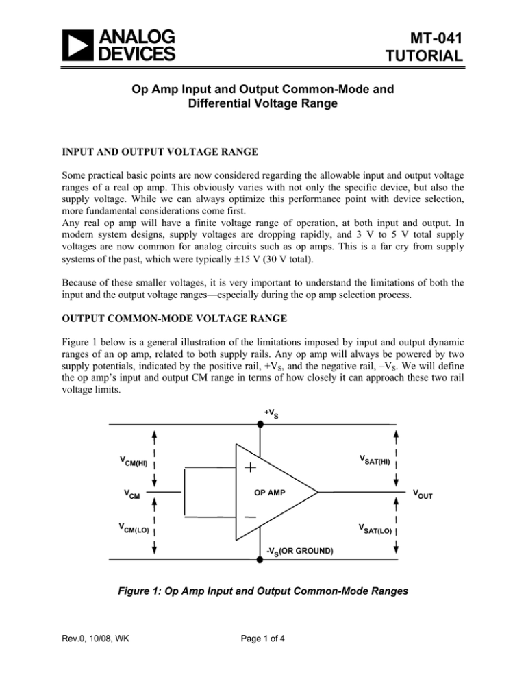
MT-041 TUTORIAL Op Amp Input and Output Common-Mode and Differential Voltage Range INPUT AND OUTPUT VOLTAGE RANGE Some practical basic points are now considered regarding the allowable input and output voltage ranges of a real op amp. This obviously varies with not only the specific device, but also the supply voltage. While we can always optimize this performance point with device selection, more fundamental considerations come first. Any real op amp will have a finite voltage range of operation, at both input and output. In modern system designs, supply voltages are dropping rapidly, and 3 V to 5 V total supply voltages are now common for analog circuits such as op amps. This is a far cry from supply systems of the past, which were typically ±15 V (30 V total). Because of these smaller voltages, it is very important to understand the limitations of both the input and the output voltage ranges—especially during the op amp selection process. OUTPUT COMMON-MODE VOLTAGE RANGE Figure 1 below is a general illustration of the limitations imposed by input and output dynamic ranges of an op amp, related to both supply rails. Any op amp will always be powered by two supply potentials, indicated by the positive rail, +VS, and the negative rail, –VS. We will define the op amp’s input and output CM range in terms of how closely it can approach these two rail voltage limits. +VS VSAT(HI) VCM(HI) VCM OP AMP VCM(LO) VOUT VSAT(LO) -VS(OR GROUND) Figure 1: Op Amp Input and Output Common-Mode Ranges Rev.0, 10/08, WK Page 1 of 4 MT-041 At the output, VOUT has two rail-imposed limits, one high or close to +VS, and one low, or close to –VS. Going high, it can range from an upper saturation limit of +VS –VSAT(HI) as a positive maximum. For example if +VS is 5 V, and VSAT(HI) is 100 mV, the upper VOUT limit or positive maximum is 4.9 V. Similarly, going low it can range from a lower saturation limit of –VS + VSAT(LO). So, if –VS is ground (0 V) and VSAT(LO) is 50 mV, the lower limit of VOUT is simply 50 mV. Obviously, the internal design of a given op amp will impact this output CM dynamic range, since, when so necessary, the device itself must be designed to minimize both VSAT(HI) and VSAT(LO), so as to maximize the output dynamic range. Certain types of op amp structures are so designed, and these are generally associated with designs expressly for single-supply systems. This is covered in more detail in Tutorial MT-035. INPUT COMMON MODE VOLTAGE RANGE At the input, the CM range useful for VIN also has two rail-imposed limits, one high or close to +VS, and one low, or close to –VS. Going high, it can range from an upper CM limit of +VS – VCM(HI) as a positive maximum. For example, again using the +VS = 5 V example case, if VCM(HI) is 1 V, the upper VIN limit or positive CM maximum is +VS – VCM(HI), or 4 V. Figure 2 below illustrates by way of a hypothetical op amp’s data how VCM(HI) could be specified, as shown in the upper curve. This particular op amp would operate for VCM inputs lower than the curve shown. VCM(HI) VCM(LO) Figure 2: A Graphical Display of Op Amp Input Common-Mode Range Page 2 of 4 MT-041 In practice the input CM range of real op amps is typically specified as a range of voltages, not necessarily referenced to +VS or –VS. For example, a typical ±15 V operated dual supply op amp would be specified for an operating CM range of ±13 V. Going low, there will also be a lower CM limit. This can be generally expressed as –VS + VCM(LO), which would appear in a graph such as Figure 2 as the lower curve, for VCM(LO). If this were again a ±15 V part, this could represent typical performance. To use a single-supply example, for the –VS = 0 V case, if VCM(LO) is 100 mV, the lower CM limit will be 0 V + 0.1 V, or simply 0.1 V. Although this example illustrates a lower CM range within 100 mV of –VS, it is actually much more typical to see single-supply devices with lower or upper CM ranges, which include the supply rail. In other words, VCM(LO) or VCM(HI) is 0 V. There are also single-supply devices with CM ranges that include both rails. More often than not however, single-supply devices will not offer graphical data such as Figure 2 for CM limits, but will simply cover performance with a tabular range of specified voltage. OP AMP DIFFERENTIAL INPUT VOLTAGE RANGE In normal operation, an op amp has the feedback loop connected; therefore the differential input voltage is held at zero volts (neglecting the offset voltage). However under certain conditions, such as power-up, the op amp may be subjected to a differential input voltage which is not zero. Certain input structures require limiting of differential input voltage to prevent damage. These op amps will generally have internal back-to-back diodes across the inputs. This will not always show up in the simplified schematics of the amps. It will show up, however, as a differential input voltage specification of ±700 mV maximum. In addition you may find a spec for the maximum input differential current. Some amps have current limiting resistors built in, but these resistors raise the noise, so for low noise op amps there are left off. The general subject of input overvoltage and protection is covered in Tutorial MT-036. OUTPUT CURRENT AND OUTPUT SHORT CIRCUIT CURRENT Most general purpose op amps have output stages which are protected against short circuits to ground or to either supply. This is commonly referred to infinite short circuit protection, since the amplifier can drive that value of current into the short circuit indefinitely. The output current that can be expected to be delivered by the op amp is the output current. Typically the limit is set so that the op amp can deliver 10 mA for general purpose op amps. If an op amp is required to have both high precision and a large output current, it is advisable to use a separate output stage (within the feedback loop) to minimize self-heating of the precision op amp. This added amplifier is often called a buffer, since it typically will have a voltage gain = 1. Page 3 of 4 MT-041 There are some op amps that are designed to give large output currents. An example is the AD8534, which is a quad device that has an output current of 250 mA for each of the four sections. A word of warning, if you try to supply 250 mA from of all four sections at the same time, you will exceed the package dissipation spec and the amp will overheat, and could destroy itself. This problem gets worse with smaller packages, which have lower dissipation. High speed op amps typically do not have output currents limited to a low value, since it would affect their slew rate and ability to drive low impedances. Most high speed op amps will source and sink between 50 - 100 mA, though a few are limited to less than 30 mA. Even for high speed op amps that have short circuit protection, junction temperatures may be exceeded (because of the high short circuit current) resulting in device damage for prolonged shorts. REFERENCES: 1. Hank Zumbahlen, Basic Linear Design, Analog Devices, 2006, ISBN: 0-915550-28-1. Also available as Linear Circuit Design Handbook, Elsevier-Newnes, 2008, ISBN-10: 0750687037, ISBN-13: 9780750687034. Chapter 1. 2. Walter G. Jung, Op Amp Applications, Analog Devices, 2002, ISBN 0-916550-26-5, Also available as Op Amp Applications Handbook, Elsevier/Newnes, 2005, ISBN 0-7506-7844-5. Chapter 1. 3. Copyright 2009, Analog Devices, Inc. All rights reserved. Analog Devices assumes no responsibility for customer product design or the use or application of customers’ products or for any infringements of patents or rights of others which may result from Analog Devices assistance. All trademarks and logos are property of their respective holders. Information furnished by Analog Devices applications and development tools engineers is believed to be accurate and reliable, however no responsibility is assumed by Analog Devices regarding technical accuracy and topicality of the content provided in Analog Devices Tutorials. Page 4 of 4


