Journal of The Electrochemical Society, 151 共7兲 C492-C494 共2004兲
C492
0013-4651/2004/151共7兲/C492/3/$7.00 © The Electrochemical Society, Inc.
Plasma Etching Transfer of a Nanoporous Pattern on a Generic
Substrate
L. Menon,a,z K. Bhargava Ram,a S. Patibandla,a D. Aurongzeb,a M. Holtz,a
J. Yun,b V. Kuryatkov,b and K. Zhub
a
Department of Physics, bDepartment of Electrical Engineering, and Nano Tech Center, Texas Tech
University, Lubbock, Texas 79409, USA
We describe a nonlithographic nanofabrication method for creating a nanoporous pattern on any substrate. The approach utilizes
plasma etching through a nanoporous template to transfer the pore pattern onto the substrate. We demonstrate this method to
transfer a porous alumina pattern consisting of a hexagonal array of 50 nm diam pores onto an aluminum layer. A nanoporous
alumina template 共0.6 m兲 is initially created by electrochemical anodization of an aluminum film 共1 m兲 deposited on a
substrate. Controlled plasma etching is then used to etch through the pores onto the aluminum layer below the pores. In this
manner, we demonstrate the hexagonal array of 50 nm diam pores in the aluminum film.
© 2004 The Electrochemical Society. 关DOI: 10.1149/1.1759973兴 All rights reserved.
Manuscript submitted October 8, 2003; revised manuscript received January 3, 2004. Available electronically June 4, 2004.
Nanoporous alumina is highly effective in the fabrication of arrays of nanometer-scale structures.1-3 An aluminum oxide membrane
is produced consisting of cylindrical arrays of nanosized pores with
diameters ranging from ⬃10-200 nm. When prepared under special
conditions, the pores can exhibit a very high level of ordering.4,5
These two factors, small feature size and high level of ordering,
make nanoporous alumina an attractive template for patterning in
nanofabrication. This approach has already been used to prepare
self-assembled nanoarrays of various materials by direct electrodeposition of the material into the pores.6,7 This has allowed both
detailed investigation of the structure of the nanoarrays and the
study of fundamental phenomena at the nanometer scale. However,
application of electrodeposited nanostructures in devices is limited,
mostly due to poor sample quality of electrodeposited nanostructures. Another problem is that the membrane is commonly grown on
commercially available aluminum foil, which limits the range of
applicability in devices.
Ideally, one would like to transfer or grow the membrane on
commercially viable substrates or epitaxial layers, such as Si, and
develop processing methods to offer various device fabrication possibilities. Several attempts have been made in this regard. Most of
these attempts have involved physical transferring of the nanoporous
alumina template onto a substrate 共the ‘‘mask’’ method兲. The nanoporous alumina template then acts as a mask through which appropriate materials can be grown inside the pores.8-10 Although the
mask method is useful for fabrication of a self-assembled nanoarray,
the area over which these nanoarrays can be grown is very small,
only of the order of a few millimeters. This is because the mask
method involves thinning of the alumina template to a thickness of
the order of 0.2-0.5 m. Aluminum oxide, being brittle, breaks up
into small pieces, of the order of a few millimeters at such a small
thickness. Hence, instead of transferring the membrane, one would
like to ‘‘grow’’ the membrane directly on a substrate. In this paper
we present an approach that allows us to grow porous alumina membranes directly on a substrate. The method also allows us to transfer
the nanopore pattern onto the substrate, which in turn increases the
versatility of the method.
The technique combines an anodization process to produce template arrays and plasma etching to reveal an intermediate layer, a
seed/adhesion layer, or the substrate. By anodizing an aluminum
film, a thin nanopore array is first created on a substrate. A major
problem for applications based on this method is posed by the etching of the thin barrier layer of alumina at the pore bottoms to pattern
layers directly below. Wet chemical etching methods, such as the use
of dilute phosphoric acid, although attempted in the past by other
research groups,11,12 are not particularly useful. In addition to re-
z
E-mail: Latika.Menon@ttu.edu
moving the barrier layer, the wet etching also causes pore widening,
thus increasing the pore diameter and in some cases completely
removing the alumina film. The directional and anisotropic attributes
of plasma etching are essential for this approach, because the template pores are small with very high aspect ratios. The etching conditions require critical control to avoid complete etching of the
membrane. In this paper, we describe chlorine plasma etching experiments for producing pores that are tens of nanometers in diam
and appear in an ordered hexagonal array.
Silicon wafers were used as the starting substrate material for
demonstrating the technique. In principle, the approach can be extended to other substrates, and we have conducted preliminary experiments on epitaxial GaN.13 Substrates are prepared using an
acetone/ethanol deionized water clean, then loaded into an E-beam
evaporator with base pressure ⬃10⫺7 mTorr. A 5 nm thick adhesion
layer of Ti 共99.98% purity starting material兲 is deposited on the Si
substrates by E-beam evaporation followed by a 1 m thick layer of
Al 共99.999% purity兲 without breaking vacuum. Without the Ti layer,
the subsequently grown membrane peels from the substrate. The
aluminum film is then anodized in an acid under dc conditions.
During anodization, aluminum is converted to nanoporous aluminum oxide. More details of the template process can be found
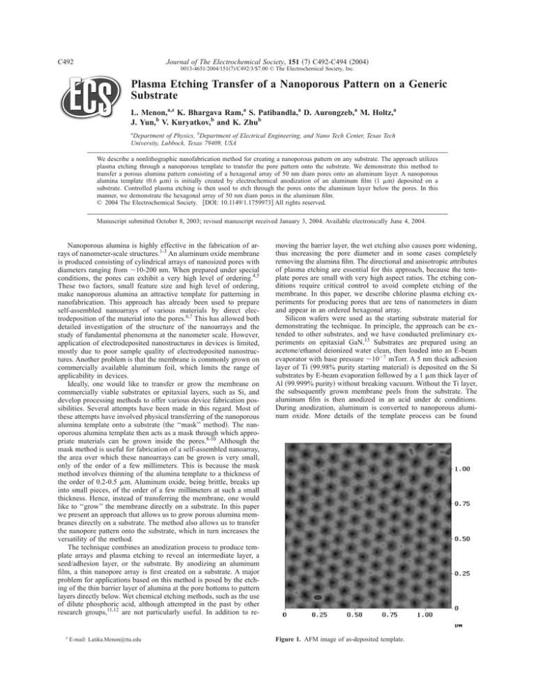
Figure 1. AFM image of as-deposited template.
Journal of The Electrochemical Society, 151 共7兲 C492-C494 共2004兲
C493
Figure 2. 共a兲 SEM cross-sectional image of as-deposited template. 共b兲 Magnified view of the same. 共c兲 SEM cross-sectional image following 60 s etch with 200
W RIE power.
elsewhere.1 The pore diameter is controlled by the anodization conditions. Anodization in 3% oxalic acid at 40 V gives a membrane
with pore diam 50 nm, as addressed here. Figure 1 shows a representative atomic force microscope 共AFM兲 image demonstrating the
regularity in pore diameter and the obtained hexagonal array.
A scanning electron microscope 共SEM兲 cross-sectional image of
the as-deposited template is shown in Fig. 2a. Clearly seen are the Ti
adhesion layer, the Al layer that remains following anodization, and
the alumina layer produced by the anodization process. The presence of a thin barrier layer of alumina 共U-shaped barrier兲 is also
seen at the pore bottoms. The thickness of the barrier layer is only of
the order of 10-20 nm. The depth of the pores in the membrane is
directly proportional to the anodization time. Here the anodization
was carried out for 2-3 min, producing a porous alumina template
⬃0.6 m thick atop the 1.0 m aluminum layer, indicating an expansion in volume.14 A magnified view is seen in Fig. 2b showing a
SEM image focusing on the barrier layer in the as-fabricated porous
alumina.
Plasma etching was carried out using a commercial inductively
coupled plasma 共ICP兲 system with reactive ion etching 共RIE兲. Cl2
diluted with Ar was used as etchant. The basic etching conditions
are given in Table I. The low chamber pressure produces conditions
of high mean-free path and high Knudsen number. These conditions
are conducive to highly directional and anisotropic etching of the
high aspect ratio 共⬃30:1兲 features. Samples were attached to quartz
wafers and loaded into the plasma reactor, where they were held to
the chuck by helium flow. The wafer temperature was not controlled; we estimate it to remain below 100°C during the etch process. The RIE power was varied from 100 to 300 W. We expect the
RIE power to be a critical parameter, because RIE has the combined
effect of redirecting etchant adhered to the top surface into the pores
and of increasing the volatility of etch by-products. Under these
processing conditions, we find Al to etch at ⬃2 m/min. The alumina barrier etches in 30-40 s, for an approximate etch rate of 60
nm/min. Under identical conditions, sapphire is completely etch resistant in 60 s. Although the addition of BCl3 etches sapphire,15 this
approach is undesirable here because the alumina template would
etch more effectively, possibly eliminating the template. Based on
the selectivity of chlorine etching to Al over alumina, the correct
etching conditions are expected to redirect etchant into the nanopore
template, break through the barrier layers of alumina, and rapidly
etch the aluminum, leaving the alumina template largely intact. Furthermore, charging of the insulating alumina results in an appreciable field at the pore opening, because ions are expected to be
readily captured near the surface due to the small pore sizes.16 The
resultant field assists channeling of ions into the high aspect ratio
features.
The etch process is highly sensitive to the etch time because of
the relative etch rates of Al and alumina. For example, etching for
30 s at 200 W RIE power is not sufficient to break through the
alumina barrier layer, although there is a reduction in total thickness
of the porous alumina layer at the top 共0.3 m兲. However, a 60 s
etch at the same 200 W RIE power is sufficient to break through the
barrier layer. Figure 2c shows SEM cross-sectional images of the
sample following a 60 s etch with 200 W RIE power. The pores in
the top nanoporous alumina layer can be clearly seen, and the alumina layer at the top is further reduced to be about 0.2 m thick. In
addition, the etch has penetrated through the barrier region and continued down through the Al to the Ti adhesion layer. Several of the
Al nanotubes produced by the process have snapped from cleaving,
showing the hexagonal shape of the parent hole template. This result
Table I. Basic etching conditions.
Plasma parameter
Value
ICP power
RIE power
Chamber pressure
Cl2 /Ar flow rates
300 W
100-300 W
8 mTorr
20/5 sccm
Figure 3. AFM image of top view of the aluminum template post removal
of the porous alumina layer (pore diam ⬃ 50-60 nm).
C494
Journal of The Electrochemical Society, 151 共7兲 C492-C494 共2004兲
shows that these conditions produce the highly directional and anisotropic etching necessary to reach the adhesion/substrate level for
extremely small features.
The etch result was also sensitive to the RIE power. For example,
a 60 s etch at a reduced 100 W RIE power is not sufficient to break
through the barrier layer. Evidently, the roles of RIE to redirect
etchant deep into the nanopores and to assist desorption of byproducts is essential. In contrast, at a higher RIE power of 300 W,
we observed ⬃200 nm removal of the alumina surface and significantly degraded morphology. Under these conditions, a 60 s etch did
not break through the barrier layer. We suggest from this that the
alumina template is physically etched 共i.e., sputtered兲 at this RIE
power. The associated surface damage sufficiently restricts the transfer of etchant into the nanopores, thereby eliminating the barrier
etch.
Following breakthrough of the barrier layer, the etch time dictates the depth of the aluminum pores, whether or not the Ti layer is
etched, and the extent of etching into the substrate. Thus, the etch
can be used to reveal several possible array structures with high
regularity for subsequent process steps. Alumina surviving the etching process can be stripped away to reveal the Al template by preferential wet etching. Figure 3 shows an AFM image of the top view
of the aluminum template post removal of the porous alumina layer
by soaking in a mixed solution consisting of 0.2 M chromic/0.4 M
phosphoric acid. The pore diam is of the order of 50-60 nm, similar
to that of the initial alumina film. We demonstrate from this that the
alumina pore pattern is directly transferred to the aluminum with no
significant degradation.
Conclusion
We have developed an approach for producing nanometer-scale
pore patterns of aluminum on silicon substrates. Pore sizes as small
as 50 nm were plasma etched with aspect ratios of ⬃30. The etch
process requires critical control over the etch time due to differing
rates of Al and alumina etch. We observed a strong dependence of
the etch on the RIE power. The process is highly versatile and appears to be restricted only by the need to produce the patterning
template from Al and alumina.
Acknowledgment
The authors acknowledge partial support for this work from the
National Science Foundation 共ECS-0070240, ECS-0323640, ECS0304224, and CTS-0210141兲.
Texas Tech University assisted in meeting the publication costs of this
article.
References
1. L. Menon, in Quantum Dots and Nanowires, H. S. Nalwa and S. Bandopadhyay,
Editors, p. 141, American Scientific Publishers, Stevenson Ranch, CA 共2003兲.
2. D. Routkevich, A. A. Tager, J. Haruyama, D. Almawlawi, M. Moskovits, and J. M.
Xu, IEEE Trans. Electron Devices, 43, 1646 共1996兲.
3. M. Moskovits and B. Schmid-Halter, Int. Pat. Wo88/02538 共1988兲.
4. H. Masuda and K. Fukuda, Science, 268, 1466 共1995兲.
5. H. Masuda, F. Hasegawa, and S. Ono, J. Electrochem. Soc., 144, L127 共1997兲.
6. M. Zheng, L. Menon, H. Zeng, Y. Liu, S. Bandyopadhyay, R. D. Kirby, and D. J.
Sellmyer, Phys. Rev. B, 62, 12282 共2000兲.
7. L. Menon, M. Zheng, H. Zeng, S. Bandyopadhyay, and D. J. Sellmyer, J. Electron.
Mater., 29, 510 共2000兲.
8. D. Crouse, Y.-H. Lo, A. E. Miller, and M. Crouse, Appl. Phys. Lett., 76, 49 共2000兲.
9. H. Masuda, K. Yada, and A. Osaka, Jpn. J. Appl. Phys., Part 2, 37, L1340 共1998兲.
10. J. Liang, H. Chik, A. Yin, and J. Xu, J. Appl. Phys., 91, 2544 共2002兲.
11. O. Rabin, P. R. Herz, S. B. Cronin, Y.-M. Lin, A. I. Akinwande, and M. S. Dresselhaus, Mater. Res. Soc. Symp. Proc., 636, D4.7.1 共2001兲.
12. Q. Huang, W.-K. Lye, D. M. Longo, and M. L. Reed, Mater. Res. Soc. Symp. Proc.,
636, D9.49.1 共2001兲.
13. L. Menon and M. Holtz, Unpublished.
14. O. Jessensky, F. Müller, and U. Gösele, Appl. Phys. Lett., 72, 1173 共1998兲.
15. C. C. Mitchell, D. D. Koleske, D. M. Follstaedt, N. A. Missert, K. H. A. Bogart, K.
Cross, M. E. Coltrin, and A. A. Allerman, 39th Symposium of the New Mexico
American Vacuum Society, p. 15, Albuquerque, NM, April 29-30, 2003.
16. W. N. G. Hitchon, Plasma Processes for Semiconductor Fabrication, p. 131, Cambridge University Press, Cambridge 共1999兲.
