Droplet Bouncing Behavior in the
advertisement
Droplet Bouncing Behavior in the
Direct Solder Bumping Process
Wayne Hsiao and Jung-Hoon Chun
Laboratory of Manufacturing and Productivity
Massachusetts Institute of Technology
Abstract— This paper presents the results of an ongoing effort
to develop a direct solder bumping process for electronics
packaging. The proposed process entails delivering molten
droplets onto specific locations on electronic devices to form
solder bumps. This study is focused on investigating droplet
deposition behaviors that affect solder bump characteristics such
as final bump volume, shape, and adhesion strength. The
occurrence of droplet bouncing has a strong influence on these
characteristics. The potential for a droplet to bounce in the
absence of solidification was modeled in discrete stages based on
energy conservation. Wetting and target surface roughness were
identified as the critical parameters affecting bouncing. The
experimental results showed that improvements in wetting and
decreases in surface roughness retard bouncing.
These
observations agreed well with the trends predicted by the energy
conservation based model. The knowledge acquired in this study
is expected to contribute to the development of an efficient solder
bumping process.
Index Terms— Droplet deposition behaviors, Droplet-based
manufacturing, Solder bumping, Electronics packaging.
I. INTRODUCTION
Several methods of producing uniform sized microdroplets
have been developed [1-3]. The Uniform Droplet Sprays
(UDS) process [1, 4], for example, is capable of producing
molten metal droplets in diameters suitable for wafer bumping
and BGA packaging applications. The ability to deliver these
droplets accurately onto specific targets has also been
demonstrated [5, 6]. However, a fundamental understanding
of droplet deposition behaviors is far from complete.
Recent studies on post-impact droplet deposition behaviors
have focused mostly on droplet spreading progression and
associated solidification phenomena [7-10]. Most of these
studies have assumed that a deposited droplet maintains
contact with the target surface continuously. However, in
some cases a deposited droplet may recoil violently after the
initial spreading and disengage from the target surface. Such
behavior, also known as bouncing, has a strong influence on
final bump volume, shape, and adhesion strength.
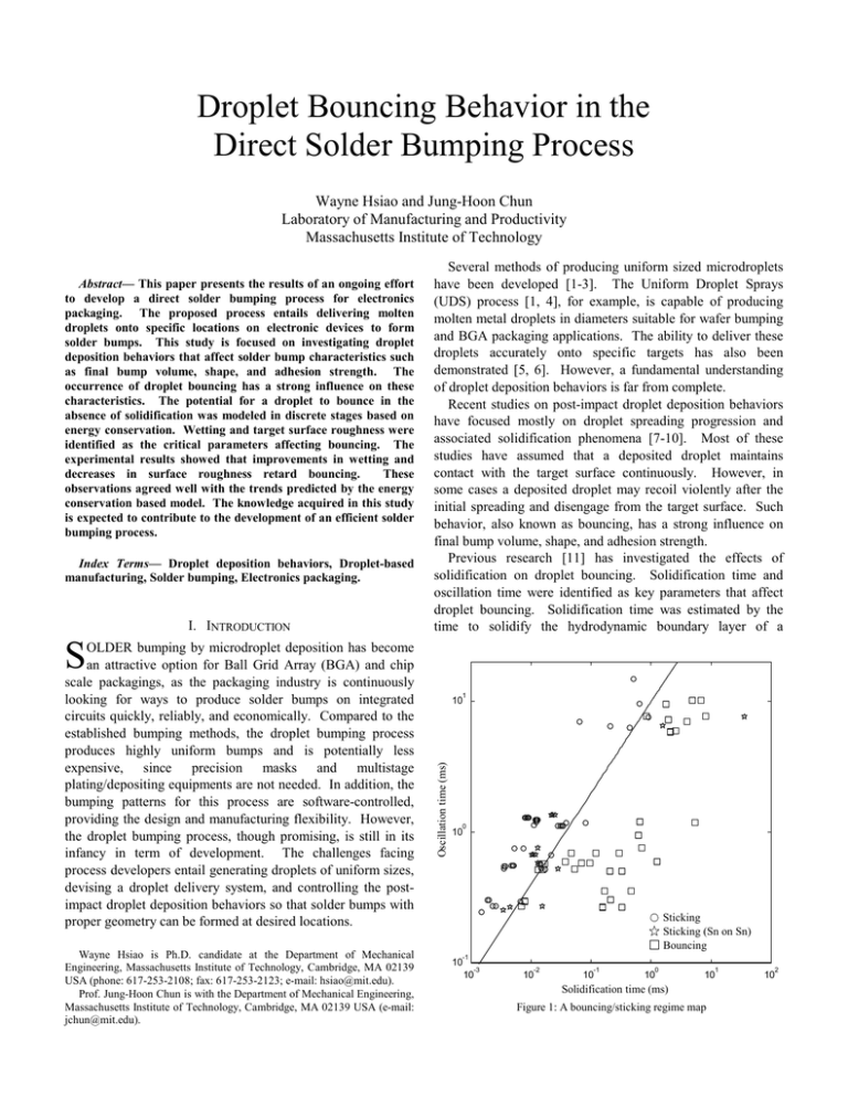
Previous research [11] has investigated the effects of
solidification on droplet bouncing. Solidification time and
oscillation time were identified as key parameters that affect
droplet bouncing. Solidification time was estimated by the
time to solidify the hydrodynamic boundary layer of a
S
Wayne Hsiao is Ph.D. candidate at the Department of Mechanical
Engineering, Massachusetts Institute of Technology, Cambridge, MA 02139
USA (phone: 617-253-2108; fax: 617-253-2123; e-mail: hsiao@mit.edu).
Prof. Jung-Hoon Chun is with the Department of Mechanical Engineering,
Massachusetts Institute of Technology, Cambridge, MA 02139 USA (e-mail:
jchun@mit.edu).
1
10
Oscillationtime
time(ms)
(ms)
Oscillation
OLDER bumping by microdroplet deposition has become
an attractive option for Ball Grid Array (BGA) and chip
scale packagings, as the packaging industry is continuously
looking for ways to produce solder bumps on integrated
circuits quickly, reliably, and economically. Compared to the
established bumping methods, the droplet bumping process
produces highly uniform bumps and is potentially less
expensive, since precision masks and multistage
plating/depositing equipments are not needed. In addition, the
bumping patterns for this process are software-controlled,
providing the design and manufacturing flexibility. However,
the droplet bumping process, though promising, is still in its
infancy in term of development. The challenges facing
process developers entail generating droplets of uniform sizes,
devising a droplet delivery system, and controlling the postimpact droplet deposition behaviors so that solder bumps with
proper geometry can be formed at desired locations.
0
10
Sticking
Sticking
Sticking
Sticking(Sn
(Snon
onSn)
Sn)
Bouncing
Bouncing
-1
10
-3
10
-2
10
-1
0
10
10
Solidificationtime
time (ms)
(ms)
Solidification
1
10
Figure 1: A bouncing/sticking regime map
2
10
deposited droplet, which was determined using a one
dimensional heat conduction model. Oscillation time was
approximated using the free oscillation period of a liquid drop.
Experiments were conducted by depositing Sn droplets onto
non-wetting surfaces, such as Al, glass, and stainless steel.
The data was used to construct a regime map, shown in Figure
1, which indicates that the tendency for droplet bouncing
decreases as the solidification time decreases. The study
therefore concluded that rapid quenching of deposited droplets
is effective in preventing bouncing on non-wetting surfaces.
However, a quenched droplet deposit typically forms a flat
splat with large diameter. Splats with these features are
unsuitable for fine pitched solder bumping applications, as
they may bridge and short closely spaced soldering pads.
Raising the target surface temperature and hence, lowering the
solidification rate, allows the deposited droplet to recoil back
to a more hemispherical shape, but the tendency for droplet
bouncing increases as the solidification time increases.
Therefore, other ways to prevent droplet bouncing need to be
explored.
Dini
V
Stage 1
Dmax
h
Stage 2
θ
Stage 3
Dini
Stage 3*
Figure 3: Stages of droplet spreading
analytical model based on energy conservation was used to
describe post-impact droplet spreading and recoiling in stages.
Parameters associated with wetting and surface roughness
were varied in the model to investigate their effects on
bouncing. An experimental study was conducted to validate
the model predictions.
II. RESEARCH FINDINGS
During the previous investigation, a change in the tendency
for droplet bouncing was observed when droplets were
deposited onto wetting surfaces. Specifically, when Sn
droplets were deposited on a freshly formed Sn surface, they
adhered to the surface, although the solidification time
suggested bouncing should occur. Further experiments have
shown that Sn droplets adhered to Au-plated Al substrates but
bounced off of bare Al substrates at the same substrate
temperature. Figure 2 shows the resultant splat morphologies
from such experiments. Therefore, in addition to solidification
time and oscillation time, these preliminary observations
suggest that wetting may also affect droplet bouncing.
Another parameter that may influence the droplet bouncing
behavior is the surface roughness of the bumping targets.
Surface roughness is known to alter the wetting condition and
the interfacial thermal contact resistance between the deposited
liquid splat and target solid [12, 13]. However, the effects of
surface roughness on droplet bouncing are not yet well
understood.
This study, therefore, aims to investigate the effects of
wetting and surface roughness on droplet bouncing. An
(a)
(b)
Figure 2: Sn splats on (a) Au-plated Al substrate at 180°C, and
(b) as-rolled Al substrate at 180°C
A. Model
Post-impact droplet spreading and recoiling behaviors can
be characterized in discrete stages based on the conservation
of energy [14]. In the current study, we adopt this model to
analyze the effects of wetting and surface roughness on
bouncing. Since we are interested in investigating the sole
roles of these liquid-substrate surface interactions in arresting
droplet bouncing, the model is simplified by assuming an
isothermal droplet deposition, i.e. no solidification. The stages
of the model are shown in Figure 3 and are described as
follows:
Stage 1 (impact): The energy of the droplet at this stage, E1,
consists of surface and kinetic energies, determined by the
initial droplet diameter, Dini, and impact velocity, V as,
E1 = SE1 + KE
(
)
2 3
= π D 2 γ lv + π ρV Dini
12
ini
(1)
where ρ and γ lv are the liquid density and the liquid-vapor
surface tensions, respectively.
Stage 2 (maximum spreading): At this stage, the outward
flow of the droplet liquid ceases and the flow front comes to a
momentary stop before recoiling. The droplet shape at this
stage resembles a cylindrical disk with diameter, Dmax, and
height, h. At this moment, the kinetic energy is zero and the
potential energy is negligible. Thus, the total energy at this
point, E2, consists of surface energy only and is represented as,
0.8
EE22*
EE2*
0.6
0.4
0.2
0
0
20
40
60
80
100 120
Contact angle
Angle(degree)
(degree)
Contact
140
160
0.4
180
E = SE 2
)
(
2
= 1 π D 2 +π D h γ lv + π Dmax γ −γ
sl
sv
max
4
4 max
)
*
)
(2)
3
Dini
2
Dmax
(
)
γ sv are often not readily available. However, γ sl −γ sv can be
estimated using Young’s equation:
sl
)
−γ sv = −γ lv cos θ
(3)
where θ is the equilibrium contact angle between the liquid
splat and the substrate surface.
By substituting Eq. (3) into Eq. (2) and normalizing Dmax
(
)
using the so-called “spread factor,” ξ max = Dmax Dini , E2 can
be written as a function of ξ max as,
2
E = π Dini γ
lv
4
2
the
(4)
(5)
energy
lost,
primarily
by
viscous
dissipation, during a deposited droplet’s initial spread to
Dmax .
Stage 3 (sticking): If the recoiling following Stage 2 does
not lead to bouncing, then the deposited droplet dissipates its
kinetic energy through oscillation until an equilibrium state is
reached. The final splat shape and its corresponding surface
energy at this state are determined by the initial droplet volume
and the equilibrium contact angle.
Stage 3* (bouncing): This stage represents the theoretical
minimum energy state when droplet bouncing occurs. The
deposited droplet is shown recoiling back to its original
spherical shape and resting just above the surface. The energy
at this stage, E3*, can be expressed as,
= SE3 + PE
(
)
= π D 2 γ lv +
ini
(7)
where Wb is the dissipation work done while a deposited
droplet recoils from its maximum spreading state.
The occurrence of droplet bouncing, therefore,
is
energetically influenced by the values of Wdiss , Wb , and E2.
An increase in dissipations during spreading and recoiling, as
well as smaller maximum spreading (lower E2), decreases the
tendency for droplet bouncing. The effects of wetting and
surface roughness on dissipations will be studied in the future.
In the current study, we investigate the influences of wetting
and surface roughness on the total energy at the maximum
spreading state, E2.
The degree of wetting can be represented by the equilibrium
contact angle, θ , in Eq. (4). A smaller contact angle correlates
to better wetting condition. As shown in Figure 4, the
*
E2 = E1 − Wdiss
*
E3
1
normalized energy, E 2 = E2 E1 , increases as θ increases.
8
2
−1
3 ξ max + ξ max (1− cos θ )
The energy conservation between Stage 1 and Stage 2 can
then be established as,
where Wdiss is
0.9
E3 = E2 − Wb
where h = 23
. γ sl and γ sv are the solid-liquid and
solid-vapor surface tensions, respectively. Values for γ sl and
(γ
0.6
0.7
0.8
Area
fraction
Area
Fraction
as,
2
(
0.5
Figure 5: Effect of area fraction on the total energy at the splat
maximum spreading state
Figure 4: Effect of contact angle on the total energy at the splat
maximum spreading state
(
1
0.8
0.6
0.4
0.2
0
π
4
ρ gDini
12
(6)
*
The energy balance between Stage 2 and Stage 3 is shown
Therefore, the model suggests that the tendency for droplet
bouncing decreases with improved wetting.
Addressing the effects of surface roughness on bouncing is a
more complicated issue. Other researchers have accounted for
the effects of surface roughness by correlating them to changes
in the equilibrium contact angle [14]. In our model, the
surface roughness effects are incorporated by applying
changes in the effective contact area under the splat. Eq. (4) is
then modified as,
(
)
2
−1
E = 1πξmax
+ 2πξmax
γ lv
2
4
3
{
(
)(
+ π ξ max Fa γ lv cos θ + 1− F γ +γ
a
lv
sv
4
2
)}
(8)
where Fa is the contact area fraction associated with the
surface roughness. The value of Fa is assumed to increase
toward unity as the surface becomes smoother. Figure 5 shows
the correlation between Fa and E2* in the case of Sn droplets
deposited onto a Au-plated surface, where γ sv
≅
1.6 N/m . The
*
figure indicates that E2 and hence, the tendency for droplet
bouncing, decreases as Fa increases.
B. Experimental Study
The droplets generated for the experimental study were
Piezo
vibrator
Crucible
θ
Sprayed droplets
Inert gas
chamber
Substrate
holder
Figure 6: Contact angle measurement
Table 1: Measured values of liquid-solid contact angle
Liquid
Solid
Contact angle
Sn
Al
95°*
Sn
Cu
42.1°
Sn
Sn (oxide)
54.4°
Sn
Ni
40.6°
Sn
Rh
35.2°
Sn
Au
28.5°
Sn
Pd
23.1°
* Estimated for non-wetting condition
produced using the UDS process. The system is capable of
producing micron-sized droplets rapidly with less than ±3%
variation in size. Therefore, the process ensured good
repeatability for our experiments, since the thermal and kinetic
states of the droplets were both predictable and controllable.
To study the effects of wetting, 3mm-thick Cu substrates
were polished using 0.3µm aluminum oxide (Al2O3) slurry in
an automatic polishing machine. The resulting smooth
surfaces eliminated surface roughness as a variable in the
wetting experiments. Different plating materials were then
applied to the substrates to vary wetting conditions for the
deposited droplets. To simulate the conditions encountered in
the actual bumping applications, typical wettable plating
materials used in electronic packaging were selected: Au, Pd,
Ni, Rh, and Sn. The semi-wetting and non-wetting conditions
were produced using polished Cu and Al substrates,
respectively. The wetting conditions were quantified by
measuring the equilibrium contact angles, θ , using the profile
images of Sn splats on these substrates, as shown in Figure 6.
The splats were made by reflowing deposited droplets in an
inert gas environment. The average values of θ for the
substrates used in the experiments are listed in Table 1. The
measured contact angle for Sn splat on Sn-plated substrate is
considerably larger than expected for homologous deposition.
The poor wetting condition is most likely caused by surface
oxidation.
To study the effects of surface roughness, 3mm-thick Cu
substrates were prepared by either sandblasting with 27µm or
180µm Al2O3 particles or by polishing with 0.3µm Al2O3
slurry. The resulting surfaces were measured to have an
average roughness, Ra, ranging from 0.02µm to 2.2µm. Ra is
defined as the arithmetic average of the deviations from the
mean height of the surface. The roughness level was chosen to
cover the range typically encountered in solder bumping
Mass-flux
measuring cup
Testing jig
Figure 7: Experimental setup
applications, from less than 0.06µm Ra for wafer UBM to
around 0.5µm Ra for BGA pads.
Post-process inspection of the sandblasted substrates
revealed that Al2O3 particles up to 5µm in size were embedded
in the soft copper surfaces. Therefore, the sandblasted
substrates were plated with a 10µm to 20µm-thick layer of
copper to ensure that the embedded particles were not exposed
prior to the final Au-plating. The substrates were then plated
with a 0.25µm-thick layer of Au to create wetting surfaces.
Both the wetting and the roughness effect experiments were
conducted using a testing jig inside an inert gas-filled chamber,
as shown in Figure 7. The testing jig was designed to hold
multiple substrates simultaneously for splat collection. The
temperature of the substrates was controlled using cartridge
heaters and thermocouples. The jig placed the substrates at
200mm below the UDS orifice. The droplets were ejected
from a 150µm orifice and had a mean diameter of 280µm.
Pure Sn was selected as the droplet material. The temperature
of the molten Sn in the crucible was maintained at 280°C. The
droplets were fully liquid and were estimated to be at 232°C
when they impacted the substrates.
The deposition
experiments were performed at substrate temperatures ranging
from 175°C to 220°C.
Determination of bouncing was made by examining the
splats collected on substrates after the deposition experiments.
Irregularly shaped splats and/or significantly lower splat
population density on substrates were used as indicators of the
occurrences of droplet bouncing.
C. Results and Discussion
Figure 8 shows the Sn splats collected on substrates with
increasing degree of wetting from (a) to (g). The surface
temperatures of all substrates were held at 200°C during
(a) Polished Al
(b) Polished Cu
(c) Ni-plated Cu
(d) Sn-plated Cu
(e) Rh-plated Cu
(f) Au-plated Cu
Figure 8(a) shows that very few splats remained on the
polished Al substrate after deposition, indicating that droplet
bouncing had occurred. The splats collected on the polished
Cu, Ni-plated, and Sn-plated substrates, as seen in Figures
8(b)-8(d), consist of mixed populations of well-adhered splats
and the remnants of bounced droplets. Clear evidence of
bouncing is shown in Figure 8(c), where circular residuals left
behind by bounced droplets can be seen on the Ni-plated
surface. Elemental analysis using an x-ray microanalyzer (Jeol
JXA-733 Superprobe) confirmed that these residuals contain a
significant amount of Sn. These observations suggest a
transition from sticking to bouncing behavior when deposits
are made on these surfaces. The splats collected on Rh-plated,
Pd-plated, and Au-plated substrates have symmetrical,
hemispherical shapes and comparable population densities, as
shown in Figures 8(e)-8(g). These characteristics indicate that
bouncing was most likely absent during depositions on these
surfaces.
To quantify the effects of wetting on droplet bouncing, the
values of E2* were estimated for the deposited droplets. The
spreading factors,
ξ max , were approximated using the
diameters of the splats collected or the circular residues when
bouncing had occurred. Examples of these measurements are
shown in Figure 9.
The average values of ξ max for the droplet deposited on
1 mm
(g) Pd-plated Cu
Figure 8: Sn splats on surfaces with different wetting properties at
Ts=200°C
collection. The lower surface temperature prevents remelting
of splats, thus preserving their morphologies.
The
characteristic solidification and oscillation times were
calculated to ensure that the depositions were made within the
bouncing regime.
these substrates are listed in Table 2. The standard deviation
for these values is less than 3%, suggesting that wetting may
not have a strong influence on the maximum spreading
diameter for the parameter ranges used in these experiments.
Similar results have been reported in other published studies
[14, 15].
Figure 10 shows that E2* decreases as the wetting condition
improves, as predicted by our model. In addition, the
experimental results confirmed that the tendency for droplet
bouncing increases as E2* increases. The figure also suggested
(a) Partial remains of Sn splats on polished Al
1 mm
(b) Sn splats and residues on Ni-plated Cu
(c) Sn splats on Pd-plated Cu
Figure 9: Estimations of the maximum spreading diameter from the collected splats
Table 2: Average values of the measured maximum
spreading diameter and the resultant spreading factors
Droplet
Sn
Sn
Sn
Sn
Sn
Sn
Sn
Target
Al
Cu
Sn (oxide)
Ni
Rh
Au
Pd
Ave. ξmax
1.80
2.09
1.91
1.96
1.95
1.94
2.04
Ave. Dmax
516µm
588µm
547µm
555µm
555µm
551µm
583µm
(a) 180µm Al2O3 blasted substrate; Ra=2.2µm
0.4
Model
Experiment: bouncing
Experiment: transition
Experiment: sticking
0.3
Al
E2*
(b) 27µm Al2O3 blasted substrate; Ra=0.4µm
0.2
Cu
Sn (oxide)
Ni
Pd
0.1
Au
Rh
0
0
10
20
30
40
50
60
70
80
90
100
Contact angle (degree)
Figure 10: Comparison between the experimental results and model
prediction of the effect of contact angle on bouncing
the existence of a bouncing/sticking transition zone between
E2* = 1.35 and E2* =2.1.
Figure 11 shows the Sn splats collected on substrates with
decreasing surface roughness. The surface temperatures of the
substrates were also kept at 200°C during the experiments.
Figure 11(a) shows that virtually no splat remained on the
180µm blasted surface, indicating that droplet bouncing might
have occurred. The splats collected on the 27µm blasted
substrate and the polished substrate have symmetrical,
hemispherical shapes and comparable population densities, as
shown in Figures 11(b) and 11(c), respectively. This suggests
that droplet bouncing might not have occurred on these
substrates.
To verify the correlation between surface roughness and the
effective contact area, a scanning electron microscope was
used to examine the droplet-surface interfaces. Figures 12(a)
and 12(b) show interfaces of splats on 180µm blasted and
27µm blasted substrates, respectively. The images were taken
at 440x magnification. The size and number of interfacial
voids increase as the surface roughness increases. These voids
effectively reduce the contact area under the splat and result in
lower Fa. Furthermore, the plated Au was observed to have
(c) Polished substrate; Ra=0.02µm
Figure 11: Sn splats on surfaces with different roughness at
Ts=220°C
diffused into the Sn splat in Figures 12(a) and 12(b). Such
regions of Au diffusion decrease in frequency and size as the
surface roughness increases. This diffusion phenomenon is an
indicator of good splat to surface contact and may be used as
an additional metric to determine the effective contact area.
Attempts are being made to extract the appropriated values of
Fa from these results and use them to quantify the effects of
surface roughness on droplet bouncing.
III. SUMMARY
An energy-based model was used to describe the mechanism
responsible for droplet bouncing.
Two parameters,
equilibrium contact angle and effective contact area, were used
to represent the effects of the droplet liquid to target solid
interactions on the bouncing behavior. As the degree of
wetting between the deposited droplet and target surface
decreases, from strong wetting on Au and Pd to nearly nonwetting on Al, the tendency for bouncing increases. Increases
in surface roughness have also been shown to promote droplet
bouncing. This phenomenon can be attributed to decreases in
(a) 180µm Al2O3 blasted substrate; Ts=175°C
(b) 27 µm Al2O3 blasted substrate; Ts=175°C
Figure 12: SEM images of interfaces between Sn splats and sandblasted surfaces
the effective contact area between the splats and the target
surfaces, as shown in the model and the experimental study.
IV. ACKNOWLEDGEMENT
The authors would like to thank the Singapore-MIT
Alliance for the financial support of this study.
REFERENCES
[1]
[2]
[3]
[4]
[5]
[6]
[7]
[8]
[9]
[10]
[11]
[12]
[13]
[14]
[15]
Yim, P., Chun, J.-H., Ando, T., and Sikka, V.K., 1996, “Production and
characterization of mono-sized Sn-Pb alloy balls,” International Journal
of Powder Metallurgy, Vol. 32, p. 155.
Tseng, A.A., Lee, M.H., and Zhao, B., 2001, “Design and operation of a
droplet deposition system for freeform fabrication of metal parts,”
Journal of Engineering Materials and Technology, Vol. 123, pp. 74-84.
Bogy, D.B. and Talke F.E., 1984, “Experimental and theoretical study
of wave propagation phenomena in drop-on-demand ink jet devices,”
IBM Journ. Res. Develop., Vl. 29, pp.314-321.
Rocha, J.C., Chun, J.-H., 1999, “Production of highly uniform solder
spheres using a digital integral control scheme,” Journal of the
International Institutions for Liquid Atomization and Spray Systems,
Vol. 9, No. 6, pp. 601-621.
Orme, M. and Bright, A., 2000, “Recent advances in highly controlled
molten metal droplet formation from capillary stream break-up with
applications to advanced manufacturing,” Liquid Metal Atomization:
Fundamentals and Practice, ed. by Cooper, K.P. et al, pp. 157-168.
Orme, M. et al, 2000, “Charged molten metal droplet deposition as a
direct write technology,” Mat. Res. Soc. Symp. Proc., Vol. 624, pp. 1822.
Waldvogel, J.M. and Poulikakos, D., 1997, “Solidification phenomena
in picoliter size solder droplet deposition on a composite substrate,” Int.
J. Heat Mass Transfer, Vol. 40, No. 2, pp. 295-309.
Xiong, B., Megaridis, C.M., Poulikakos, D., and Hoang, H., 1998, “An
investigation of key factors affecting solder microdroplet deposition,”
Journal of Heat Transfer, February, 1998, Vol. 120, pp. 259-270.
Aziz, S.D. and Chandra, S., 2000, “Impact, recoil and splashing of
molten metal droplets,” Int. J. Heat Mass Transfer, Vol 43, pp. 28412857.
Pasandideh-Fard, M., Bhola, R., Chandra, S., and Mostaghimi, J., 1998,
“Deposition of tin droplets on a steel plate: simulations and
experiments,” Int., J. Heat Mass Transfer, Vol. 41, pp. 2929-2945.
Kim, H.-Y., 1999, “Spreading behavior of molten metal microdroplets,”
Ph.D. thesis, Massachusetts Institute of Technology, Cambridge, MA,
USA.
Nakae, H., Inui, R., Hirata, Y., and Saito, H., 1998, “Effects of surface
roughness on wettability,” Acta Mater., Vol. 46, No. 7, pp. 2313-2318.
Wang, G.-X. and Matthys, E.F., 1996, “On the heat transfer at the
interface between a solidifying metal and a solid substrate,” in Melt
Spinning, Strip Casting and Slab Casting, ed. by Matthys, E.F. and
Truckner, W.G., The Minerals, Metals & Materials Society, pp. 205236.
Mao, T., Kuhn, D.C.S., and Tran, H., 1997, “Spread and rebound of
liquid droplets upon impact on flat surfaces,” AIChE Journal, Vol. 43,
No. 9, pp. 2169-2179.
Scheller, B.L., and Bousfield, D.W., 1995, “Newtonian Drop Impact
with a Solid Surface,” AIChE J., Vol. 41, No. 6, pp. 1357-.
