IV. SOLID-STATE MICROWAVE ELECTRONICS*,
advertisement
IV.
SOLID-STATE MICROWAVE ELECTRONICS*,
Academic and Research Staff
Prof. P. Penfield, Jr.
Prof. D. H. Steinbrecher
V. C. Howey
Graduate Students
J.
J.
D. F. Peterson
H. P0
A.
E. Rudzki
R. Selin
THEORETICAL SMALL-SIGNAL ANALYSIS OF AN
AVALANCHE DIODE IN THE s-PLANE
1.
The oretical-Impedance Calculation
of Fig. IV-1,
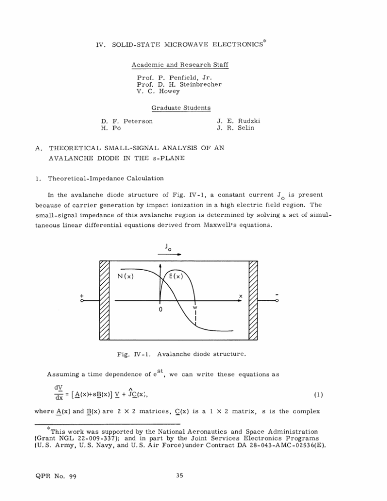
In the avalanche diode structure
a constant current Jo is present
because of carrier generation by impact ionization in a high electric field region. The
small-signal impedance of this avalanche region is determined by solving a set of simultaneous linear differential equations derived from Maxwell's equations.
Jo
Fig. IV-i.
Avalanche diode structure.
st
Assuming a time dependence of est,
dV
-d
we can write these equations as
A
(1)
= [A(x)+sB(x)] V + JC(x),
where A(x) and B(x) are 2 X 2 matrices, C(x) is
a
1 X 2 matrix,
s is the complex
This work was supported by the National Aeronautics and Space Administration
(Grant NGL 22-009-337); and in part by the Joint Services Electronics Programs
(U.S. Army, U.S. Navy, and U.S. Air Force)under Contract DA 28-043-AMC-02536(E).
QPR No. 99
(IV.
SOLID-STATE MICROWAVE ELECTRONICS)
A
frequency variable o + j w, and J is the amplitude of the total small-signal current in
the diode.
The vector V(x) comprises the small-signal electric field amplitude and the
small-signal hole current amplitude.
That is,
E(x)
(2)
.
V(x) =
The elements of the matrices A,
B, and C depend on x through the static electric
field and hole and electron concentrations.
These static values are found by solving the
nonlinear static form of Maxwell's equations for the diode,
given the doping N(x) and
the DC current J , in a special computer subroutine that has been written by Professor
1 o
Paul Penfield.
In his analysis, the hole and electron ionization coefficients and carrier
velocities have their standard experimentally determined form.
Equation 1 must be solved under the boundary conditions that at the left edge of the
avalanche region (x=0),
A
J (0) = 0,
(3)
and at the right edge of the region (x=w),
A
J n(w) = 0,
(4)
A
where the electron current J (x) is given by
A
A
A
Jn(X) = J - J p(x) - s
A
E(x).
(5)
The width w of the avalanche region is determined by the doping profile N(x) and the
direct avalanche current J
o
The boundary conditions can be satisfied by considering the solution of (1) as
V = XVh + Vi,
(6)
A
where V
h
is the homogeneous solution of (1),
Vh(O)
(J=0), with
K]
(7)
A
V
1
is the inhomogeneous solution of (1),
V.(0) =
QPR No. 99
0
1011
(J=1), with
(8)
(IV.
SOLID-STATE MICROWAVE ELECTRONICS)
and X is a complex constant to be determined.
Boundary condition (3) is thus satisfied
for any choice of X.
By using the initial conditions (7) and (8), the solutions for Vh(x) and Vi(x) can be
generated by iteration across the avalanche region at equally spaced points Ax apart.
The value of Ax can be made as small as desired, but was usually chosen as w/100. The
multiplier X is determined from the values of V h(w) and V.(w) combined with the boundh
ary condition (4).
A
-1
From (5), we have
A
A
Jnh(w) = -Jph(w) - s
Eh(w)
-[1 sE] V h(w)
(9)
and
J
.(w)= 1 - [1 SE] V.i(w),
ni
-1
(10)
A
Then (4) requires
since J = 1.
A
A
A
J (w)
Jnh (w) + J ni(w) = 0
or
k
1 - [1 SE] Vi(w)
[1
(11)
sE] V h(w)
A
Equation 11 fails if J
A
nh
(w) = 0, but this only happens if both boundary conditions are sat-
isfied with J = 0, or when the value of s used in the calculation is an open-circuit natural frequency.
A
The small-signal voltage amplitude V is obtained from integration of the electric
A
field E(x) from x = 0 to x = w, and the impedance is then given as
A
Z(s) = V(s),
(12)
A
since J = 1.
By following the procedure above for many values of s, we can generate
the impedance throughout the s-plane.
In the rest of this report, the diode admittance
will be analyzed because this makes the data both easier to handle and readily comparable to the admittance of a circuit model.
The particular diode used in this study was a one-dimensional silicon diffused type
with a background doping of 1021/m
3 .
Its admittance had the pole-zero pattern of
Fig. IV-2 at each of the values of bias current tested, being unstable for both shortcircuit and open-circuit conditions at the terminals of the avalanche region.
As Jo varied, the zero locations moved considerably, while the pole frequency
remained essentially fixed on the real axis.
QPR No. 99
A searching
routine
was written to
(IV.
SOLID-STATE MICROWAVE
ELECTRONICS)
os
s -plane
o
a
p
Fig. IV-2.
Pole-zero pattern of calculated admittance.
accurately determine these frequencies.
Figure IV-3 shows their movement in the
s-plane for values of bias J. between 104 A/ m 2 and 10 6 A/m2
14 -
=
J
6
10
5
7 x 10
5 x 10
5
5
3x 10
5
2 x 10
5
J = 10
4
7x 10
5x 10⁴
4
3x 10
4
2x 10
SIGMA ( Grad/s)
Fig. IV-3.
Natural frequencies of the avalanche
region vs bias.
The computed admittance will now be compared with that of a simple circuit model
that has the same pole-zero pattern.
This is accomplished by comparing constant con-
tours of the real and imaginary parts of the calculated admittance with those of the
QPR No. 99
(IV.
SOLID-STATE MICROWAVE ELECTRONICS)
circuit admittance in a normalized-frequency plane.
2.
Circuit Model for the Avalanche Diode
a.
Model Characteristics
The
proposed
circuit
model for
the
diode
is
shown
-
Fig. IV-4.
in
Fig.
IV-4.
The
C
Circuit model for avalanche diode.
admittance of this circuit is
1 - rg + s(rc-fg) + s 2c
yd(s) =
(13)
r + st
and has the same pole-zero pattern as Fig. IV-2,
1
ri ±
1
V1c
1
4T
with the zeros at
4 + r
-c
(14)
and the pole at
(15)
=: -r/f
where in this case r will be negative.
z = x + jy = sN-t+
where
QPR No. 99
-,
If a new frequency variable z is defined as
(16)
(IV.
SOLID-STATE
x = (r+r/f) - \
MICROWAVE ELECTRONICS)
c
(17)
and
Y ==W\-
,
(18)
then (13) can be written
yd(z)
d(z)
1
+ y = z +
(19)
where
1/2
(20)
and
S= g/Yo+
(21)
rY
Normalized and shifted in this way, Yd(z) is the universal impedance of the circuit, since
it does not depend on any of the circuit-element values. In the z-plane, Yd(z) can be
modeled as a parallel combination of an inductance and a capacitance,
one,
so the pole is now at z = 0 and the zeros at ±j 1.
each with value
This is shown in Fig. IV-5.
jY
Sso
s- plane
j 1
z - plane
P
A
-
0
0 S*
Fig.
IV-5.
Impedance transformation from s-plane to z-plane.
Constant conductance
by setting
QPR No. 99
and susceptance contours in the z-plane are determined
(IV.
d = x
Re
2
+ 2
1x +y
SOLID-STATE MICROWAVE ELECTRONICS)
n = const.
(22)
m = const.
(23)
and
Im {yd} =
-
2
x
x +y
Each choice of m and n defines a curve in the z-plane,
orthogonal to curves of constant Im {Yd}.
with curves of constant Re {Ud}
The first quadrant of such a plot is shown in
Fig. IV-6, where the susceptance is odd about the x-axis and even about the y-axis, and
the conductance is odd about the y-axis and even about the x-axis.
1.5
1.0
n=0.5
2.0
3.0
2.5
3.3
m
3.0
3
d
2.85
Yo
2.5
Gd
n
2.414
Yo
12
2.0 Yo g )112
'2 +
2
)1 /2
Y,
~.5
1.617
1.281
1.0
0.781
0.5
m=0
0.617
0.414
0.35
0.30
m= -0.5
0
2
1
0.38
2.62
3
x, ( + )Ac
Fig. IV-6.
b.
Constant Re {yd} and Im {yd} contours
in the z-plane.
Normalization of Calculated Admittance
Figure IV-6 serves as a reference with
compared.
QPR No. 99
Operations
equivalent
to Eqs.
which the computed admittance
16-21
will be
for the computed admittance are
(IV.
SOLID-STATE MICROWAVE
determined at each value of J
o
ELECTRONICS)
from the pole and zero frequencies
o-' and s'.
o
p
These
equivalent operations are
p
z' = x' + jy' =-
o
op
a-
(24)
p
(T
p
X'
(25)
=
(26)
(27)
2
( ' --s 'I
(28)
o
p
and
S Po
+%)
yd(z') =
+
Y',
(29)
',
where cd is considered to be a known quantity that is equal to the avalanche region capacThe primes refer to quantities defined from the calculated
itance per unit area, E/w.
data.
Again, the pole is at z' = 0 and the zeros at z' =
+j 1, as shown in Fig. IV-7.
z'- plane
s - plane
0
S
I
0
jI
(I
P
p
S-
pl
-j 1
s
o
Fig. IV-7.
QPR No. 99
Impedance transformation from s-plane to z'-plane.
SOLID-STATE
(IV.
c.
ELECTRONICS)
MICROWAVE
Comparison of Calculated Data with Reference Data
The contours of constant Re
{yd} and
Im
{jj} were
determined from computation of
(29) after the pole and zero frequencies had been determined in a separate calculation.
For a given contour value and a given x' value, the y' value was found
by
a
searching
At one value of bias (105 A/m2), the y' values were determined for several
routine.
values of x' for all values of the reference contours specified in Fig.
IV-6.
In each
case the y' value agreed with the reference y value to at least 3 decimal places.
At
the other values of Jo' only the contour intercepts along the x' and y' axes were checked
These results show that the diode can be
and the agreement was also as good.
accurately
modeled by the circuit of Fig. IV-4 if we choose the element values cor-
rectly. This choice was already made by stating equivalence of Eqs. 16-21 to Eqs. 2429,
which is equivalent to matching pole and zero frequencies of both admittances with
c = cd .
The model element values are thus given as
g = ( 2 o- -)c
(30)
d
P
p
(31)
=
r=
cd s'
'
-
2
cdL
o+
(0-o
2
1
(32)
cd
+
( Go-o
- )2
and
(33)
c = cd.
Table IV-1 shows the actual admit-
As further verification of the model's validity,
tance values vs the equivalent circuit admittance values evaluated along the jw axis. At
a frequency of approximately 10 times the resonant frequency, the two sets of data
begin to disagree, and the model is no longer valid.
d.
Bias Dependence
To complete the modeling of the diode, we must include the bias dependence of the
admittance along with its frequency dependence.
Since the pole and zero frequencies
can easily be found at several values of bias current Jo, the dependence of the circuit
element values on Jo can readily be determined from Eqs. 30-33. The movement in
the s-plane of the natural frequencies vs bias was seen in Fig. IV-3,
QPR No. 99
and Fig. IV-8 is
Table IV-1.
Frequency response of calculated admittance
and equivalent-circuit admittance.
ck t. (
calc.
om'1a
e
calc.
0O 0
0E
1')31E
10310
1
I,00
0
270CE O
10l31E
1051E
1031E
l
50
0 E
1000
0
0
50() E
3300
U030F
E
1331
1031E
1031E
1031E
1031E
1051E
1031E
9000 E
i o 0o E
00
O
0
O
O
3000E
1031E 0
1031E
103i E 0
1030E 0
i )0 E
7 000
0 0 rE
1030E
1030E
1020E
!029E
1024E
1015E
1003E
0874E
1 691E
79 E
5 )0 E
9269E 0
1 ()
00 E
()
0E
7000E
9
(1000
2000EE
300EE
- 3 0
4 C)
') 0 00 E
00O
1172E
9483E
7882E
0
0
0
0412E
0.
1353E
lb 24E
1240E
102340
210 E
2435E
2706E
54I12E
01160
iII2E
1352E
1iG22E
1892E
210E
2430E )
0.
G.
O1
0.
0:
U:.
:
0.
01
Of
O0
O
0'
0'
5416L
c124 E
1303E
11
11
11
11
11
ii
12
1625E
1391E
21bUE I
2437E I
2708E
5416E
0122E
1083E I
1353E
1031E
1331E
1031E
1030 E
103 t) E
103OE
1029E
10 24 E
LO 15E
1003E
O
T
0
0
'695E
0
j4 f 0E
1010EE 0.
19
01
2050E O
1810E 01
1312E O1
1965E 01O
131 L
194lE
40'350
lG2E
0152E
100E
119E
13770
1436E
1173E
'490E
7890E
-.
1724E
0[
.358E
06
-.
-.
-.
-.
-.
-.
-.
1894E
2523E
2700E
2402E
1835E
3085E
04
04
04
04
04
03
.7973E
.9589E
.1121
.1282E
.1i444E
.1(05E
06
-.
-.
-.
-.
-.
-.
6711E
I
I
(
1
1
1
3091E I
2739E
1967E
G94E
i
1261E
i4U E
1652E
1811E
1944E
2r4025E
76 E
1008E 0'
11 5 E 01
1377E 01
3092E 0
4735E 01
06
07
07
07
07
2700E
5355E
7910E
9021 E
2720E
1945E
3000E
i031E
iL03
1E
1031E
1031E
S1031 E
2698E O
)351 E 0
7913E
1034 E
12 GIE
!2 7 E
1650E
000 U E
U
0
0
0
(1
0
0
5702E
QPR No. 99
0
0
0
0
0
SW1i2E
.031E
1031E
0O,
9 3' E 01
80 0 E
900OE
.5000E
.6000E
.7000E
.8000E
.9000E
.1000E
0
9)20E 0
8763E 0)
u059E 0
4 G2GE 0)
2763EE
19 9E 0
1000 E
.409i)E
O
E
ckt . B
4735E
O
1567E 04
1498E04
1457E 04
1429E 04
1411E 04
1396E 04
. u359E
06
.797bE
.9589E
.1120E
.1281E
.1442E
.1602E
OU
U
07
07
07
07
I
I i
I I
I ,
I
I
1
1 1
11
-4
5
10
_
10
5
4
10-
10
E
z
E
3
10
10-6
2
-
10
10 71
6
5
4
10
10
10
A/ m2
J (
DIRECT
CURRENT
Fig. IV-8.
1
10 A/
H-rn2
P=(4.16/J 0 )xl0 106
circus bias Jt.
Equivalent-circuit elements
c
=
1.605 x 10- 5 F/m
.34J x 10
£=(4.16/Jo)
104 A/m2 (J
r = -0.983/J J o
Fig. IV-9.
QPR No. 99
Diode equivalent circuit.
2
2
mhos/m2
10
x
10-
0-
<10 6 A/m
-m
H-m
2
(IV.
SOLID-STATE MICROWAVE
ELECTRONICS)
a log-log plot of the corresponding element values r,
remains nearly constant,
to J.
f,
and g vs J .
Since o- = -r/f
o
P
r and k vary together and appear to be inversely proportional
The conductance g is proportional to J , while c remains essentially constant
over the test range in bias 10
A/
m
< J
< 10 6 A/
m
The complete
circuit model
2
is thus shown in Fig. IV-9, where the admittance is in mhos/m , since all calculations
o
.
were made on a unit area basis.
3.
Conclusions
The small-signal admittance of an avalanche diode calculated directly from Maxwell's
equations can be modeled by a simple four-element circuit in a region of the s-plane
that includes the natural frequencies.
The bias dependence of the admittance is charac-
terized by the dependence of the element values on the direct current J .
This simple
model can be easily handled by existing circuit-analysis computer programs and is use-
ful in design of microwave active circuits.
One should recognize that the model only characterizes the region of the diode in
which impact ionization is taking place and the electric field is high, and does not include
effects occurring in the high-conductivity,
low electric field inactive end regions.
D. F.
References
1.
P.
Penfield, Jr. , Private communication, August 1970.
QPR No. 99
Peterson

