Chapter 5. Subsurface Charge Accumulation Imaging
advertisement
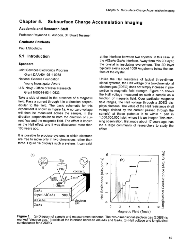
--- - -~b4~ I ~~ Chapter 5. Subsurface Charge Accumulation Imaging Chapter 5. Subsurface Charge Accumulation Imaging Academic and Research Staff Professor Raymond C.Ashoori, Dr. Stuart Tessmer Graduate Students Paul I.Glicofridis 5.1 Introduction Sponsors Joint Services Electronics Program Grant DAAH04-95-1-0038 National Science Foundation Young Investigator Award U.S. Navy - Office of Naval Research Grant N00014-93-1-0633 Take a slab of metal in the presence of a magnetic field. Pass a current through it in a direction perpendicular to the field. The basic schematic for this experiment is shown in Figure la. A nonzero voltage will then be measured across the sample, in the direction perpendicular to both the direction of current flow and the magnetic field. The effect is known as the Hall effect, and it was discovered more than 100 years ago. at the interface between two crystals: in this case, at the AIGaAs-GaAs interface. Away from this 2D layer, the crystal is insulating everywhere. The 2D layer typically exists about 1000 Angstroms below the surface of the crystal. Unlike the Hall resistance of typical three-dimensional systems, the Hall voltage of a two-dimensional electron gas (2DEG) does not simply increase in proportion to magnetic field strength. Figure lb shows the Hall voltage measured on such a sample as a function of magnetic field. Over particular magnetic field ranges, the Hall voltage through a 2DEG displays plateaus. The value of the Hall resistance (Hall voltage divided by the current passed through the sample) at these plateaus is to within 1 part in 1,000,000,000 h/ie 2, where i is an integer. This stunning observation, first made about 17 years ago, has led a large community of researchers to study the effect. It is possible to produce systems in which electrons are free to move only in two dimensions rather than three. Figure la displays such a system. It can exist .i,- c (b) E -C 0 , 0 0 0 U) U c 0( _0 ! - c 0 C U) U) , C 2: c 0 2 4 6 8 0 _j0 1 Magnetic Field (Tesla) Figure 1. (a) Diagram of sample and measurement scheme. The two-dimensional electron gas (2DEG) is marked "electron gas." It exists at the interface between AIGaAs and GaAs. (b) Hall voltage and longitudinal conductance for a 2DEG. -~- - Chapter 5. Subsurface Charge Accumulation Imaging While theoretical pictures have been developed for the electronic structure in the 2DEG that gives rise to the effect, no technique allowed direct imaging of the charge distribution inside the quantum Hall fluid. Several years ago, we started to build a new type of microscope which could look beneath the surface of semiconductors. The results reveal the behavior of a strongly interacting quantum mechanical fluid of electrons. While some of the data display structure predicted by theory, a myriad of beautiful and unexpected formations also appear. While the transverse or "Hall" resistance of the 2DEG displays plateaus, the conductance between any two points within the 2D layer (longitudinal conductance) also has a very interesting behavior as the magnetic field strength is varied. The behavior of the longitudinal conductance as a function of magnetic field is plotted as the dotted curve in Figure 1 b. At the magnetic field values for which the Hall resistance displays plateaus, the longitudinal conductance becomes very small, tending to zero as the temperature of the sample is reduced to zero. The 2DEG conducts electricity only along its edges. The two experimental signatures, zeros of the longitudinal conductance and plateaus in the Hall resistance, are inextricably linked in theoretical explanations of the quantum Hall effect. Some understanding of the quantum Hall effect can be gained by considering the effect of magnetic field on noninteracting electrons. Classical electrons in a perpendicularly applied magnetic field in a 2DEG will move in circles with the "cyclotron frequency" w,=eB/ mc, where e is the charge on the electron, B is the magnetic field strength, m is the mass of the electron and c is the speed of light. Quantum mechanically, these orbits give rise to discrete energy levels known as "Landau levels." The energy difference between Landau levels is hwc, and each Landau level can contain a certain number of electrons per unit 2DEG area. This number increases with proportion to the magnetic field strength. As the field is increased, higher Landau levels depopulate, and the Landau level filling factor v decreases. Landau levels contain both spin up and spin down electrons. When the magnetic field is adjusted so that exactly one Landau is filled and fully occupied with both spin up and spin down electrons, the filling factor is v-=2. If two levels are filled, then v=4, etc. It is at integer values ofv that the plateaus in the Hall resistance are observed. 90 RLE Progress Report Number 140 A simple model can explain some of the basic features in the quantum Hall effect. Most simply, when v is near an integer value, all electronic states are filled up to an energy gap (a gap of ho. in the case of even values of v, and a "spin-gap" for odd values of v). The situation can be seen somewhat analogously to a filled valence band in an insulator. With no available states for conduction at the Fermi level, electrical conduction cannot take place. This explains the minima in the longitudinal conductance. The only place where the longitudinal conductance is not zero is at the sample edges where the density is lower, and Landau levels are therefore not completely filled. The quantized values of the Hall conductance can then be explained by the requirement that all net currents in the sample must flow at the sample edges. Amazingly, the conductance of the edges is quantized with a value which depends only on the number of Landau levels filled in the bulk. This situation leads to the observed quantized values of the Hall resistance and the Hall plateaus. If one accounts for the fact that there are local density fluctuations within the bulk, then small regions of the bulk may be conducting or insulating. As the magnetic field is varied within a range near integer values of v, a percolation transition is thought to occur. With fields close to integer values ofv, no conducting pathway exists from one edge of the sample to the other, and the longitudinal conductance drops to zero. We set out to observe this percolation transition. To our great surprise, our images did not display the transition in the sense that we expected. We spent several years building the microscope to try to observe the electronic structure giving rise to the quantum Hall effect. The microscope has proven to be a very flexible instrument. We use it to scan a tip within 50 Angstroms of the sample surface. The microscope can successfully find the sample surface, characterize the surface topography, image static charges on the sample surface, and operate in the novel capacitance mode which permits observation of structure underneath the sample surface. The microscope operates immersed in a bath of liquid helium-3 at a temperature of 0.3 K and inside a magnet capable of fields of up to 12 Tesla. The basic measurement scheme is shown in Figure la. A small ac excitation voltage is applied to a contact to the 2DEG. As the 2DEG has capacitance to a ground plane about 0.5 mm away, charge moves into Chapter 5. Subsurface Charge Accumulation Imaging and out of the 2DEG in synchrony with the ac excitation. More or less charge will accumulate in different regions of the 2DEG depending on the local conductivity of the regions and whether or not a pathway exists for charging this region from the contact. The tip of a scanning probe microscope is placed just above the surface of the sample. The tip is attached to a highly sensitive charge sensor capable of sensing one hundredth of an electron charge on the tip. The output of the sensor is fed into a synchronous detector, and for each position of the tip, the amplitude of the charge appearing in and out of phase with the excitation is measured. We call this technique subsurface electronic structure microscopy (SESM). As a first experiment, we used the microscope first to locally alter the properties density of electrons in the 2DEG, and then we use SESM to image where charge accumulates within the 2DEG. By first applying a large (4 Volt) voltage on the tip, we can use the tip (in a fashion somewhat like a field emitter) to dump negative charge on the sample surface. The surface then remains charged, even when the tip voltage is brought back to zero. The negative charge on the surface repels electrons underneath, and the density of electrons under this position is then reduced. The SESM images shown in Figure 2 are of a region where we have used this technique to lower the electron density in the region at the center of the image. The images are of an area of 2.7 microns by 2.7 microns, and there exists a broad density minimum at the center of the image. The images of Figure 2 show a SESM image of this region as the magnetic field strength is changed. An interesting and partly explainable progression occurs in the images of Figure 2. For a field of 1.0 Tesla, the sample appears metallic everywhere, and charge accumulates equally well (to the limits of our detection) everywhere underneath the surface. However, when the field is raised to 1.5 Tesla, a black spot appears in the image. A black spot indicates a region where charge does not accumulate. As the magnetic field is raised, the black spot grows. What's going on? 1.5 T 1.0 T 2.0 T Schematic arc filaments arc island droplets filaments 2.995 T 3.010 T Figure 2. (top row) SCA images of a region of perturbed 2DEG for different magnetic field strengths. (bottom row) SCA images and schematic of an unperturbed region of the 2DEG in the quantum Hall regime. Chapter 5. Subsurface Charge Accumulation Imaging These images validate some of the ideas discussed above. Recall that a region containing a filled Landau level is a poor conductor. At 1.5 Tesla, the region at the very center of the image contains one filled Landau level (v=2), and it does not accumulate charge. As the field is increased, the Landau level can contain more electrons. As the density of electrons grows as one moves away from the center of the image, the position at which exactly one Landau level is filled also moves away from the image center as the field is raised. This explains the growth of the black spot with field, but the center of the black spot has less than one Landau level filled, and it should conduct. If the interior of the black spot is conducting, why doesn't it accumulate charge? The answer is simple. Everywhere at the borders of the black spot. the 2DEG is nonconducting. Therefore, charge cannot penetrate to the interior, and the center of the spot appears black in our images, despite the fact that it likely conducts electrons. Apparently, some of the basic ideas about regions of filled Landau levels are correct, at least when a large density perturbation exists. The results of Figure 2 now establish our ability to detect separate conducting and nonconducting regions within the 2DEG The question now to be answered is: what happens in an unperturbed region as the magnetic field is adjusted to place the sample in the quantum Hall regime? Does the percolation model work? The percolation model would suggest that as the magnetic field is adjusted toward an integer value of v, black spots should appear in the images. The black spots should merge and coalesce as the field approaches integer v. Eventually, the whole picture should go black as the percolation transition will be complete and no charge can enter the sample. This is not at all what we observe! We see no evidence for black spots merging to impede conduction across the sample. We have produced a series of 36 images taken as the magnetic field is stepped in small increments through a quantum Hall plateau for v=4. The field range was from 2.96 to 3.14 Tesla in steps of only 0.005 Tesla. Even though the field was only being changed by about 1 part in 600 per step, the images changed radically with each step. At the lowest fields (outside the region of a Hall plateau), the images were featureless, indicating that all regions of the 2DEG charge equally well in response to the ac excitation. As the field is raised, structure 92 RLE Progress Report Number 140 becomes apparent. The transition into the quantum Hall plateau appears as clouds which disperse rather than black spots merging. Once the clouds disperse, underlying structure and local patterns of charging become visible. Figure 2 (bottom row) shows two capacitance images taken at fields differing by only 150 Gauss. Once again, bright regions are areas of high charge accumulation, and dark regions accumulate less charge. Notice the interesting structure in the images and their very rapid evolution with magnetic field. The images are completely stable over time. even though the field evolution is so pronounced. We observe some features which are in general agreement with the simple ideas outlined above. As the field is raised some of the bright and bulbous "islands" (see schematic) shrink in size and finally disappear. These regions likely contain electrons in higher Landau levels. As the field is increased, the higher Landau levels depopulate, and the number of electrons contained in the islands diminishes. Most other observed features do not agree with the simple ideas. Rather than shrinking, some bright regions appear to stretch and "tear" as the field strength is increased. These regions are often bordered by narrow filaments (see schematic). Indeed, many filaments can be seen throughout the picture. What are they? Three years ago, Professor Xiao-Gang Wen at MIT and graduate student Claudio Chamon postulated that such filaments could exist at the edge of a 2DEG. They arise due to exchange effects in the electron gas. As with Hund's rules in atomic physics, exchange produces correlations between electron motion in spatially nearby quantum levels. These correlations produce an effective short range attraction between electrons. Of course, the long range Coulomb repulsion remains. Under certain circumstances, electrons can actually clump and form filaments. Apparent signatures of this type of filament formation have been seen in experiments from Professor Marc Kastner's group. Our images indicate that this type of filament formation is much more prevalent than previously imagined. Other "arcs" and circular structures are clearly apparent in the images. A careful look at the image for 2.995 Tesla in Figure 2 reveals a series of concentric rings in the upper right hand corner of the image. In fact, movies made from a sequence of images reveal "cyclones" and other features which appear almost Chapter 5. Subsurface Charge Accumulation Imaging as coherent weather patterns. These features are completely unexpected. There is no known physics that produces coherent structures (such as the rings in Figure 2) on such a large (several micron) length scale in the 2DEG. The images have revealed that the essential features of the quantum Hall effect likely cannot be understood using single simple particle physics arguments. This may seem an obvious statement as electrons clearly interact strongly. However, for the sake of simplicity, the single particle model has been widely used to attempt explain experiments over the last 15 years. Now effort will be needed to understand the observed microscopic structure and how this structure leads to the quantum Hall effect as it is observed in transport experiments. After many years, the 2DEG remains a fascinating and somewhat mysterious system. Aside from allowing us to image the structure creating the quantum Hall effect, we believe that our microscope will be of other practical and scientific use. We have been working closely with Professor Leonid Levitov at MIT to understand the precise meaning of the images that we see. It is clear that we can now "look" beneath surfaces with unprecedented spatial and spectroscopic resolution. Even single electrons can be observed to enter single traps deep inside a semiconductor. A technologically important interface is the one between silicon and silicon oxide. Most transistors performing digital logic operations do so by modulating conduction at this interface. Their performance is impeded by centers which trap electrons and inhibit conduction through the layer. Our subsurface electronic structure microscope exposes the possibility of allowing one to "peer" underneath the surface and observe the mechanisms which enhance or deteriorate the performance of devices. 5.2 Publications Berman, D., R.C. Ashoori, and H.I. Smith. "Single Electron Transistors for Charge Sensing in Semiconductors." Proceedings of the International Conference on Quantum Devices and Circuits. Imperial College Press, 1997, pp. 217-23. Berman, D., N.B. Zhitenev, R.C. Ashoori, H.I. Smith, and M.R. Melloch. "The Single-Electron Transistor as a Charge Sensor for Semiconductor Applications." J. Vac. Sci. Tech. 15(6): 2844-47 (1997). Chan, H.B., P.I. Glicofridis, R.C. Ashoori, and M.R. Melloch. "Universal Linear Density of States for Tunneling into the Two-Dimensional Electron Gas." Phys. Rev Lett. 79: 2867-70 (1997). Tessmer, S.H., P.I. Glicofridis, R.C. Ashoori, and M.R. Melloch. "Subsurface Charge Accumulation Imaging of the Quantum Hall Effect." Nature. Forthcoming. Zhitenev, N.B., R.C. Ashoori, L.N. Pfeiffer, and KW. West. "Periodic and Aperiodic Bunching in the Addition Spectra of Quantum Dots." Phys. Rev. Lett. 79: 2308-11 (1997). 94 RLE Progress Report Number 140
