LT1568 Very Low Noise, High Frequency Active RC, Filter Building Block
advertisement
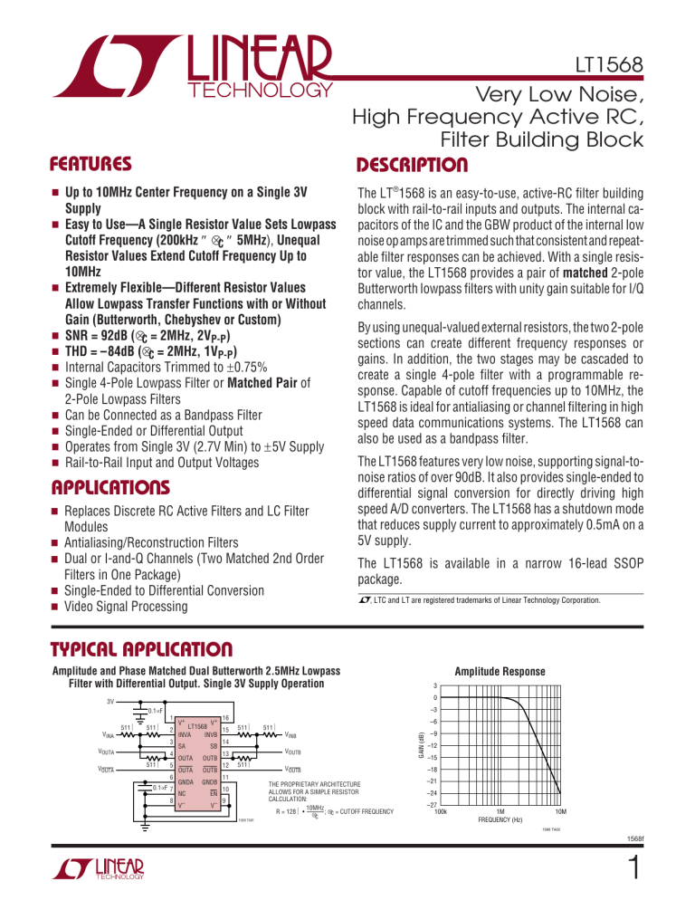
LT1568 Very Low Noise, High Frequency Active RC, Filter Building Block DESCRIPTIO U FEATURES ■ ■ ■ ■ ■ ■ ■ ■ ■ ■ ■ Up to 10MHz Center Frequency on a Single 3V Supply Easy to Use—A Single Resistor Value Sets Lowpass Cutoff Frequency (200kHz ≤ ƒC ≤ 5MHz), Unequal Resistor Values Extend Cutoff Frequency Up to 10MHz Extremely Flexible—Different Resistor Values Allow Lowpass Transfer Functions with or Without Gain (Butterworth, Chebyshev or Custom) SNR = 92dB (ƒC = 2MHz, 2VP-P) THD = –84dB (ƒC = 2MHz, 1VP-P) Internal Capacitors Trimmed to ±0.75% Single 4-Pole Lowpass Filter or Matched Pair of 2-Pole Lowpass Filters Can be Connected as a Bandpass Filter Single-Ended or Differential Output Operates from Single 3V (2.7V Min) to ±5V Supply Rail-to-Rail Input and Output Voltages U APPLICATIO S ■ ■ ■ ■ ■ Replaces Discrete RC Active Filters and LC Filter Modules Antialiasing/Reconstruction Filters Dual or I-and-Q Channels (Two Matched 2nd Order Filters in One Package) Single-Ended to Differential Conversion Video Signal Processing The LT®1568 is an easy-to-use, active-RC filter building block with rail-to-rail inputs and outputs. The internal capacitors of the IC and the GBW product of the internal low noise op amps are trimmed such that consistent and repeatable filter responses can be achieved. With a single resistor value, the LT1568 provides a pair of matched 2-pole Butterworth lowpass filters with unity gain suitable for I/Q channels. By using unequal-valued external resistors, the two 2-pole sections can create different frequency responses or gains. In addition, the two stages may be cascaded to create a single 4-pole filter with a programmable response. Capable of cutoff frequencies up to 10MHz, the LT1568 is ideal for antialiasing or channel filtering in high speed data communications systems. The LT1568 can also be used as a bandpass filter. The LT1568 features very low noise, supporting signal-tonoise ratios of over 90dB. It also provides single-ended to differential signal conversion for directly driving high speed A/D converters. The LT1568 has a shutdown mode that reduces supply current to approximately 0.5mA on a 5V supply. The LT1568 is available in a narrow 16-lead SSOP package. , LTC and LT are registered trademarks of Linear Technology Corporation. U TYPICAL APPLICATIO Amplitude and Phase Matched Dual Butterworth 2.5MHz Lowpass Filter with Differential Output. Single 3V Supply Operation Amplitude Response 3 0 3V –3 0.1µF 511Ω VINA 2 3 VOUTA VOUTA 4 511Ω 5 6 0.1µF 7 8 16 V+ LT1568 15 INVA INVB 14 SA SB 13 OUTA OUTB 12 OUTA OUTB 11 GNDA GNDB 10 NC EN 9 V– V– V+ 511Ω –6 511Ω VINB GAIN (dB) 1 511Ω VOUTB 511Ω 1568 TA01 VOUTB –9 –12 –15 –18 THE PROPRIETARY ARCHITECTURE ALLOWS FOR A SIMPLE RESISTOR CALCULATION: 10MHz R = 128Ω • ; ƒC = CUTOFF FREQUENCY ƒ C –21 –24 –27 100k 1M FREQUENCY (Hz) 10M 1568 TA02 1568f 1 LT1568 W W W AXI U U ABSOLUTE RATI GS U U W PACKAGE/ORDER I FOR ATIO (Note 1) Total Supply Voltage (V + to V –) ........................... 11.6V Input Voltage on INVA, INVB, GNDA and GNDB Pins ....................................................... V + to V – Input Current on INVA, INVB, GNDA and GNDB Pins (Note 2) ........................................... ±10mA Output Short-Circuit Duration on OUTA, OUTB, OUTA and OUTB Pins ............................................... Indefinite Maximum Continuous Output Current (Note 3) DC ............................................................... ±100mA Specified Temperature Range (Note 9) LT1568C ............................................ – 40°C to 85°C LT1568I ............................................. – 40°C to 85°C Junction Temperature .......................................... 150°C Storage Temperature Range ................ – 65°C to 150°C Lead Temperature (Soldering, 10 sec)................. 300°C ORDER PART NUMBER TOP VIEW V+ 1 16 V + INVA 2 15 INVB SA 3 14 SB OUTA 4 13 OUTB OUTA 5 12 OUTB GNDA 6 11 GNDB NC 7 10 EN V– 8 9 LT1568CGN LT1568IGN GN PART MARKING V– 1568 1568I GN PACKAGE 16-LEAD PLASTIC SSOP TJMAX = 150°C, θJA = 135°C/W Consult LTC Marketing for parts specified with wider operating temperature ranges. ELECTRICAL CHARACTERISTICS The ● denotes the specifications which apply over the full operating temperature range, otherwise specifications and typical values are at TA = 25°C. VS = single 5V, EN pin to logic “low,” RL = 400Ω, connected to midsupply, RFIL = R11 = R21 = R31 = R12 = R22 = R32, unless otherwise noted (see Block Diagram). SYMBOL PARAMETER VS Total Supply Voltage IS Supply Current VS = 3V VS = 5V VS = ±5V ● ● ● Shutdown Supply Current VS = 3V, VEN = 2.4V VS = 5V, VEN = 4.4V VS = ±5V, VEN = 4.4V ● ● ● Output Voltage Swing High (OUTA, OUTA, OUTB, OUTB Pins) VS = 3V, RFIL = 1.28k, RL = 1k VS = 5V, RFIL = 1.28k, RL = 1k VS = 5V, RFIL = 128Ω, RL = 400Ω VS = ±5V, RFIL = 1.28k, RL = 1k ● ● ● ● Output Voltage Swing Low (OUTA, OUTA, OUTB, OUTB Pins) VS = 3V, RFIL = 1.28k, RL = 1k VS = 5V, RFIL = 1.28k, RL = 1k VS = 5V, RFIL = 128Ω, RL = 400Ω VS = ±5V, RFIL = 1.28k, RL = 1k ● ● ● ● IOUT CONDITIONS MIN ● TYP 2.7 2.75 4.60 4.50 4.60 MAX 11 V 24 26 28 35 36 38 mA mA mA 0.3 0.5 1.0 1.0 1.3 2.5 mA mA mA 2.85 4.80 4.65 4.75 0.05 0.07 0.20 V V V V 0.12 0.15 0.40 –4.7 ±80 Maximum Output Current UNITS V V V V mA Op Amp Input Offset Voltage VS = 3V VS = 5V VS = ±5V ● ● ● –2.5 –2.5 –2.0 –0.5 0.2 1.2 1.5 2.5 4.5 mV mV mV Inverter Output Offset Voltage VS = 3V VS = 5V VS = ±5V ● ● ● –2 –10 –12 2.5 0.6 –4.0 7.0 4.5 2.0 mV mV mV 1568f 2 LT1568 ELECTRICAL CHARACTERISTICS The ● denotes the specifications which apply over the full operating temperature range, otherwise specifications and typical values are at TA = 25°C. VS = single 5V, EN pin to logic “low,” RL = 400Ω, connected to midsupply, RFIL = R11 = R21 = R31 = R12 = R22 = R32, unless otherwise noted (see Block Diagram). SYMBOL PARAMETER CONDITIONS MIN IB Op Amp Input Bias Current VS = 3V VS = 5V VS = ±5V ● ● ● Inverter Gain (Sections A and B, Note 5) Frequency = DC Frequency = 2MHz Frequency = 10MHz ● Inverter Phase Shift (Sections A and B, Note 5) Frequency = DC Frequency = 2MHz Frequency = 10MHz Inverter Bandwidth (Note 4) Slew Rate (OUTA, OUTB, OUTA, OUTB) Pins VCM Common Mode Input Voltage Range (GNDA and GNDB Pins, Note 6) VS = 3V VS = ±5V Single Supply GND Reference Voltage VS = 5V, GNDA Tied to GNDB EN Input Logic Low Level VS = 3V, 5V or ±5V EN Input Logic High Level VS = 3V, 5V or ±5V VIH tEN 0.5 0.4 –0.2 2 2 2 –0.2 0.01 0.01 0.27 UNITS µA µA µA MHz 0.2 dB dB dB 180 179 176 DEG DEG DEG 53 V/µs 1 to 1.9 –3.4 to 2.7 V V 2.5 ● V V + – 2.1 ● EN Input Pull-Up Resistor tDIS MAX 55 SR VIL TYP V+ V – 0.6 30 V 40 kΩ Disable (Shutdown) Time EN Pin Steps from 0V to V+ 20 µs Enable (Start-Up) Time EN Pin Steps from V+ to 0V 100 µs FILTER ELECTRICAL CHARACTERISTICS Specifications are for the output (OUTA or OUTB) of a single 2nd order section (A or B) with respect to VGND = VGNDA = VGNDB, gain = –1, RFIL = R11 = R21 = R31 = R12 = R22 = R32, (see Block Diagram). The ● denotes the specifications which apply over the full operating temperature range, otherwise specifications and typical values are at TA = 25°C. VS = single 5V, EN pin to logic “low,” RL = 400Ω, unless otherwise noted. SYMBOL PARAMETER CONDITIONS ADC DC Gain VOS(OUT) DC Offset Voltage (VOUTA – VGNDA) or (VOUTB – VGNDB) VS = 3V, fC = 1MHz, RFIL = 1.28k VS = 5V, fC = 1MHz, RFIL = 1.28k VS = ±5V, fC = 1MHz, RFIL = 1.28k ∆VOS(OUT) DC Offset Voltage Mismatch (VOUTA – VGNDA) – (VOUTB – VGNDB) VS = 3V, fC = 1MHz, RFIL = 1.28k VS = 5V, VS = ±5V, fC = 1MHz, RFIL = 1.28k MIN TYP MAX UNITS ● –1.01 –1 –0.99 V/V ● ● ● –5 –10 –12 2.6 0.6 –4.0 15 10 4 mV mV mV ● ● –8 –10 ±4 ±4 8 10 mV mV ● 0.2 Transfer Function Characteristics for Each Section (A or B) to Single-Ended Output (OUTA or OUTB) fC Cutoff Frequency Range (Note 7) TC Cutoff Frequency Temperature Coefficient VS = 3V, VS = 5V, VS = ±5V ● 10 ±1 MHz ppm/°C 1568f 3 LT1568 FILTER ELECTRICAL CHARACTERISTICS Specifications are for the output (OUTA or OUTB) of a single 2nd order section (A or B) with respect to VGND = VGNDA = VGNDB, gain = –1, RFIL = R11 = R21 = R31 = R12 = R22 = R32, (see Block Diagram). The ● denotes the specifications which apply over the full operating temperature range, otherwise specifications and typical values are at TA = 25°C. VS = single 5V, EN pin to logic “low,” RL = 400Ω connected to midsupply, unless otherwise noted. SYMBOL THD PARAMETER CONDITIONS MIN TYP MAX UNITS Filter Gain, fC = 1MHz, VS = 5V, RFIL = 1.28k (Measured with Respect to DC Gain) Test Frequency = 300kHz (0.3 • fC) Test Frequency = 750kHz (0.75 • fC) Test Frequency = 1MHz (1 • fC) Test Frequency = 2MHz (2 • fC) Test Frequency = 4MHz (4 • fC) ● ● ● ● –0.05 –1.45 –3.60 –13.7 0.05 –1.20 –3.20 –13.2 –25.0 0.25 –0.85 –2.80 –12.5 dB dB dB dB dB Filter Gain, fC = 10MHz, VS = 5V, RFIL = 128Ω (Measured with Respect to DC Gain) Test Frequency = 1MHz (0.1 • fC) Test Frequency = 7.5MHz (0.75 • fC) Test Frequency = 10MHz (1 • fC) Test Frequency = 20MHz (2 • fC) Test Frequency = 40MHz (4 • fC) ● ● ● ● –0.1 –1.5 –3.5 –14.2 0.02 –1.0 –3.0 –13.2 –27.5 0.25 –0.50 –2.40 –12.2 dB dB dB dB dB Filter Gain Mismatch (VOUTA – VOUTB) fC = 1MHz, fIN = fC fC = 10MHz, fIN = fC ● ● –0.25 –0.30 ±0.02 ±0.02 0.25 0.30 dB dB Wideband Output Noise fC = 1MHz, RFIL = 1.28k, BW = 2MHz fC = 10MHz, RFIL = 128Ω, BW = 20MHz 18 34 Total Harmonic Distortion fC = 1MHz, RFIL = 1.28k, fIN = 200kHz, VIN = 1VP-P – 84 dB fC = 10MHz, RFIL = 128Ω, fIN = 2MHz, VIN = 1VP-P – 69 dB µVRMS µVRMS Specifications are for the OUTA or OUTB of a single 2nd order section (A or B) with respect to VGND = VGNDA = VGNDB, gain = 1, RFIL = R11 = R21 = R31 = R12 = R22 = R32, (see Block Diagram) The ● denotes the specifications which apply over the full operating temperature range, otherwise specifications and typical values are at TA = 25°C. VS = single 5V, EN pin to logic “low,” RL = 400Ω connected to midsupply, unless otherwise noted. SYMBOL PARAMETER ADC DC Gain VOS(OUT) DC Offset Voltage (VOUTA – VGNDA) or (VOUTB – VGNDB) ∆VOS(OUT) DC Offset Voltage Mismatch (VOUTA – VGNDA) – (VOUTB – VGNDB) CONDITIONS MIN TYP MAX UNITS ● 0.99 1 1.01 V/V VS = 3V, fC = 1MHz, RFIL = 1.28k VS = 5V, VS = ±5V, fC = 1MHz, RFIL = 1.28k ● ● –9 –10 –2 –1 5 10 mV mV VS = 3V, fC = 1MHz, RFIL = 1.28k VS = 5V, VS = ±5V, fC = 1MHz, RFIL = 1.28k ● ● –8 –10 ±2 ±2 8 10 mV mV ● 0.2 10 MHz Transfer Function Characteristics for Each Section (A or B) to Single-Ended Output (OUTA or OUTB) fC Cutoff Frequency Range (Note 7) TC Cutoff Frequency Temperature Coefficient Filter Gain, fC = 1MHz, VS = 5V, RFIL = 1.28k (Measured with Respect to DC Gain) VS = 3V, VS = 5V, VS = ±5V ±1 ● Test Frequency = 300kHz (0.3 • fC) Test Frequency = 750kHz (0.75 • fC) Test Frequency = 1MHz (1 • fC) Test Frequency = 2MHz (2 • fC) Test Frequency = 4MHz (4 • fC) ● ● ● ● –0.10 –1.40 –3.50 –13.7 0.15 –1.00 –3.10 –13.0 –25.0 ppm/°C 0.40 –0.65 –2.60 –12.5 dB dB dB dB dB 1568f 4 LT1568 FILTER ELECTRICAL CHARACTERISTICS Specifications are for the OUTA or OUTB of a single 2nd order section (A or B) with respect to VGND = VGNDA = VGNDB, gain = 1, RFIL = R11 = R21 = R31 = R12 = R22 = R32, (see Block Diagram) The ● denotes the specifications which apply over the full operating temperature range, otherwise specifications and typcial values are at TA = 25°C. VS = single 5V, EN pin to logic “low,” RL = 400Ω connected to midsupply, unless otherwise noted. SYMBOL THD PARAMETER CONDITIONS MIN TYP MAX UNITS Filter Gain, fC = 10MHz, VS = 5V, RFIL = 128Ω (Measured with Respect to DC Gain) Test Frequency = 1MHz (0.1 • fC) Test Frequency = 7.5MHz (0.75 • fC) Test Frequency = 10MHz (1 • fC) Test Frequency = 20MHz (2 • fC) Test Frequency = 40MHz (4 • fC) ● ● ● ● –0.3 –1.2 –3.1 –12.2 0.15 –0.50 –2.30 –11.2 –19.1 0.5 0.0 –1.5 –10.2 dB dB dB dB dB Filter Gain Mismatch (VOUTA – VOUTB) fC = 1MHz, fIN = fC fC = 10MHz, fIN = fC ● ● –0.4 –0.5 ±0.02 ±0.02 0.4 0.5 dB dB Wideband Output Noise fC = 1MHz, RFIL = 1.28k, BW = 2MHz fC = 10MHz, RFIL = 128Ω, BW = 20MHz 22 60 µVRMS µVRMS Total Harmonic Distortion fC = 1MHz, RFIL = 1.28k, fIN = 200kHz, VIN = 1VP-P – 84 dB fC = 10MHz, RFIL = 128Ω, fIN = 2MHz, VIN = 1VP-P – 75 dB Specifications are for the differential output (OUTA – OUTA or OUTB – OUTB) of a single 2nd order section (A or B), gain = –2, RFIL = R11 = R21 = R31 = R12 = R22 = R32. All voltages are with respect to VGND = VGNDA = VGNDB. The ● denotes the specifications which apply over the full operating temperature range, otherwise specifications and typical values are at TA = 25°C. VS = single 5V, EN pin to logic “low,” RLDIFF = 800Ω connected at midsupply, unless otherwise noted. SYMBOL PARAMETER CONDITIONS MIN TYP MAX ADC DC Gain VOS(OUT) DC Offset Voltage (OUTA – OUTA) or (OUTB – OUTB) VS = 3V, fC = 1MHz, RFIL = 1.28k VS = 5V, fC = 1MHz, RFIL = 1.28k VS = ±5V, fC = 1MHz, RFIL = 1.28k ● ● ● –4 –12 –20 6 2 –5 16 15 10 mV mV mV ∆VOS(OUT) DC Offset Voltage Mismatch (OUTA – OUTA) – (OUTB – OUTB) VS = 3V, fC = 1MHz, RFIL = 1.28k VS = 5V, fC = 1MHz, RFIL = 1.28k VS = ±5V, fC = 1MHz, RFIL = 1.28k ● ● ● –8 –12 –15 2 –2 2 8 12 15 mV mV mV –2 ● UNITS V/V Transfer Function Characteristics for Each Section (A or B) to Differential Output (OUTA – OUTA or OUTB – OUTB) fC Cutoff Frequency Range (Note 7) TC Cutoff Frequency Temperature Coefficient VS = 3V, VS = 5V, VS = ±5V ● 0.2 10 ±1 ● MHz ppm/°C Filter Gain, fC = 1MHz, VS = 5V, RFIL = 1.28k (Note 8) (Measured with Respect to DC Gain) Test Frequency = 300kHz (0.3 • fC) Test Frequency = 750kHz (0.75 • fC) Test Frequency = 1MHz (1 • fC) Test Frequency = 2MHz (2 • fC) Test Frequency = 4MHz (4 • fC) ● ● ● ● –0.05 –1.40 –3.60 –13.7 0.10 –1.10 –3.20 –13.1 –25.0 0.25 –0.80 –2.70 –12.5 dB dB dB dB dB Filter Gain, fC = 10MHz, VS = 5V, RFL = 128Ω (Note 8) (Measured with Respect to DC Gain) Test Frequency = 1MHz (0.1 • fC) Test Frequency = 7.5MHz (0.75 • fC) Test Frequency = 10MHz (1 • fC) Test Frequency = 20MHz (2 • fC) Test Frequency = 40MHz (4 • fC) ● ● ● ● –0.20 –1.30 –3.30 –13.1 0.1 –0.8 –2.6 –12.1 –24.3 0.30 –0.20 –1.90 –11.1 dB dB dB dB dB 1568f 5 LT1568 FILTER ELECTRICAL CHARACTERISTICS Specifications are for the differential output (OUTA – OUTA or OUTB – OUTB) of a single 2nd order section (A or B), gain = –2, RFIL = R11 = R21 = R31 = R12 = R22 = R32. All voltages are with respect to VGND = VGNDA = VGNDB. The ● denotes the specifications which apply over the full operating temperature range, otherwise specifications and typical values are at TA = 25°C. VS = single 5V, EN pin to logic “low,” RLDIFF = 800Ω connected to midsupply, unless otherwise noted. SYMBOL THD PARAMETER CONDITIONS Filter Gain Mismatch (VOUTA – VOUTA) – (VOUTB – VOUTB) fC = 1MHz, fIN = fC fC = 10MHz, fIN = fC Wideband Output Noise fC = 1MHz, RFIL = 1.28k, BW = 2MHz fC = 10MHz, RFIL = 128Ω, BW = 20MHz 36 88 Total Harmonic Distortion fC = 1MHz, RFIL = 1.28k, fIN = 200kHz, VIN = 1VP-P – 84 dB fC = 10MHz, RFIL = 128Ω, fIN = 2MHz, VIN = 1VP-P – 69 dB Note 1: Absolute Maximum Ratings are those values beyond which the life of the device may be impaired. Note 2: The inputs of each op amp are protected by back-to-back diodes. If either differential input voltage exceeds 1.4V, the input current should be limited to less than 10mA. Note 3: A heat sink may be required to keep the junction temperature below the absolute maximum rating when the output is shorted indefinitely. Note 4: The inverter bandwidth is measured with the SA or SB output floating, and is defined as the frequency at which the phase shift from OUTA (OUTB) to OUTA (OUTB) drops from 180° to 135°. Note 5: Measured with the SA or SB output connected in the filter application circuit as shown in the Block Diagram. Note 6: The common mode input voltage range is measured by shorting the filter input to the common mode reference (GNDA or GNDB) and applying a DC input voltage to search for the common mode voltage range that creates a ±2mV (VS = 3V) or ±5mV (VS = ±5V) change in the (OUTA or OUTB) voltage (measured with respect to GNDA or GNDB). ● ● MIN TYP MAX UNITS –0.3 –0.4 ±0.10 ±0.15 0.3 0.4 dB dB µVRMS µVRMS Note 7: The minimum cutoff frequency of the LT1568 is arbitrarily listed as 200kHz. The limit is arrived at by setting the maximum resistor value limit at 6.4k. Due to input bias current, the output DC offset through a single section can be as high as 25mV with resistors this large. The LT1568 can be used with even larger resistors if the large offset voltages can be tolerated. For cutoff frequencies below 200kHz, refer to the LTC1563-2, LTC1563-3. Note 8: With equal-sized resistors, the differential DC gain through either a single section or cascaded sections is 6dB. Note 9: The LT1568C is guaranteed to meet specified performance from 0°C to 70°C. The LT1568C is designed, characterized and expected to meet specified performance from –40°C to 85°C but is not tested or QA sampled at these temperatures. The LT1568I is guaranteed to meet specified performance from –40°C to 85°C. 1568f 6 LT1568 U W TYPICAL PERFOR A CE CHARACTERISTICS Crosstalk vs Frequency fCUTOFF = 1MHz Supply Current vs Temperature 40 –50 –80 VIN = 2VP-P VS = 5V –85 –60 30 VS = 3V CROSSTALK (dB) VS = ±5V VS = 5V 25 VIN = 2VP-P VS = 5V OUTA, OUTB –90 CROSSTALK (dB) ICC (mA) 35 Crosstalk vs Frequency fCUTOFF = 10MHz –95 –100 OUTA, OUTB –105 –70 –80 OUTA, OUTB –90 –110 OUTA, OUTB 20 –100 –115 50 0 25 TEMPERATURE (°C) 75 85 1k 10k 100k 1M FREQUENCY (Hz) 10M Distortion vs Frequency VS = ±5V, fCUTOFF = 5MHz –40 RL = 400Ω –45 fIN = 2.5MHz RL = 400Ω –50 VIN = 1VP-P –65 –50 2ND –75 –80 3RD DISTORTION (dB) DISTORTION (dB) DISTORTION (dB) –55 –70 –60 –65 –70 2ND –75 –80 –85 2ND –70 3RD –75 –90 1M 10M 1 0 2 3 4 5 6 7 OUTA (VP-P) 8 1568 G05 70 RL = 400Ω fIN = 2.5MHz –40 –50 DISTORTION (dB) –55 –60 –65 2ND –75 –50 –60 2ND –70 3RD 3RD Power Supply Rejection vs Frequency POWER SUPPLY REJECTION (dB) –30 RL = 400Ω –45 fIN = 2.5MHz 9 10 11 1568 G06 Distortion vs Output Voltage Swing VS = 3V, fCUTOFF = 5MHz –40 DISTORTION (dB) –65 FREQUENCY (Hz) Distortion vs Output Voltage Swing VS = 5V, fCUTOFF = 5MHz –80 –60 –85 –90 500k 1568 G04 –70 –55 –80 3RD –85 5M 100M Distortion vs Output Voltage Swing VS = ±5V, fCUTOFF = 5MHz –45 1M FREQUENCY (Hz) 1M 10M FREQUENCY (Hz) 1568 G03 Distortion vs Frequency VS = ±5V, fCUTOFF = 10MHz RL = 400Ω VIN = 2VP-P –90 200k 100k 1568 G02 1568 G01 –60 –110 10k –120 15 –40 –25 –80 60 50 OUTA, OUTB 40 OUTA, OUTB 30 20 10 –85 –90 –90 0 1 2 3 4 OUTA (VP-P) 5 6 1568 G07 0 1 2 OUTA (VP-P) 3 4 1568 G08 0 10k 100k 1M 10M FREQUENCY (Hz) 100M 1568 G09 1568f 7 LT1568 U U U PI FU CTIO S V+ (Pins 1, 16): The V+ positive supply voltage pins should be tied together and bypassed with a 0.1µF capacitor to an adequate analog ground plane using the shortest possible wiring. INVA, INVB (Pins 2, 15): Inverting Input. Each of the INV pins is an inverting input of an op amp. Note that the INV pins are high impedance, and are susceptible to coupling of unintended signals. External parasitic capacitance on the INV nodes will also affect the frequency response of the filter sections. For these reasons, printed circuit connections to the INV pins must be kept as short as possible. SA, SB (Pins 3, 14): Summing Pins. These pins are a summing junction for input signals. Stray capacitance on the SA or SB pins may cause “small” frequency errors of the frequency response near the cutoff frequency (or center frequency). The three external resistors for each section should be located as close as possible to the SA or SB pin to minimize stray capacitance (one picofarad of stray capacitance may add up to 0.1% frequency error). OUTA, OUTB (Pins 4, 13): Lowpass Output. These pins are the rail-to-rail outputs of op amps. Each output is designed to drive a nominal net load of 400Ω and 30pF. OUTA, OUTB (Pins 5, 12): These pins are the inverted versions of the OUTA and OUTB outputs respectively. Each output is designed to drive a nominal load of 400Ω and 30pF. GNDA (Pin 6): GNDA serves as the common mode reference voltage for section A. It should be tied to the analog ground plane in a dual supply system. In a single-supply system, an internal resistor divider can be used to establish a half-supply reference point. In that case, GNDA must be bypassed to V– (Pins 8, 9) by a 0.1µF capacitor. NC (Pin 7): This pin is not connected internally and can be connected to ground. V– (Pins 8, 9): The V– negative supply voltage pins should be tied together and bypassed to GND by a 0.1µF capacitor in a dual-supply system. In a single-supply system, tie these pins to the ground plane. EN (Pin 10): ENABLE. When the EN input goes high or is open circuited, the LT1568 enters a shutdown state which reduces the supply current to approximately 0.5mA (VS = 5V). The OUTA, OUTB, OUTA and OUTB pins assume high impedance states. GNDA will continue to be biased at half-supply. If an input signal is applied to a complete filter circuit while the LT1568 is in shutdown, some signal will normally flow to the output through passive components around the inactive IC. EN is connected to V+ through an internal pull-up resistor of approximately 40k. This defaults the LT1568 to the shutdown state if the EN pin is left floating. Therefore, the user must connect the EN pin to a voltage equal to or less than (V + – 2.1)V to enable the part for normal operation. (For example, if V+ is 5V, then to enable the part the EN pin voltage should be 2.9V or less.) GNDB (Pin 11): GNDB serves as the common mode reference voltage for section B. It should be tied to the analog ground plane in a dual supply system. In a singlesupply system, GNDB can be tied to GNDA to set the common mode voltage at half-supply. If it is tied to another reference voltage, GNDB should be bypassed to V– (Pins 8, 9) by a 0.1µF capacitor. 1568f 8 LT1568 U U U PI FU CTIO S Dual Supply Power and Ground Connections ANALOG GROUND PLANE Single Supply Power and Ground Connections ANALOG GROUND PLANE V+ 1 16 V+ V+ 15 INVA INVB 14 SA SB LT1568 13 OUTA OUTB 12 OUTA OUTB 11 GNDA GNDB 10 NC EN 9 V– V– 2 3 4 5 6 7 8 V– V+ 1 2 0.1µF 3 4 5 6 7 0.1µF 8 16 V+ V+ 15 INVA INVB 14 SA SB LT1568 13 OUTA OUTB 12 OUTA OUTB 11 GNDA GNDB 10 NC EN 9 V– V– 0.1µF 0.1µF SINGLE POINT SYSTEM GROUND SINGLE POINT SYSTEM GROUND DIGITAL GROUND PLANE (IF ANY) DIGITAL GROUND PLANE (IF ANY) 1568 PF01 1568 PF02 U W BLOCK DIAGRA A D TEST CIRCUIT V+ CBP1 0.1µF R11 1.27k INA V+ R31 1 1.27k INVA 2 16 15 C1A SA 3 – – R21 1.27k A1A + + + OUTA A-SIDE DIFFERENTIAL OUTPUTS – OUTA OUTA R12 1.27k INB R22 1.27k 14 SB A1B 13 4 5 R32 INVB 1.27k C1B OUTB OUTB –1 –1 12 + B-SIDE DIFFERENTIAL OUTPUTS C2B C2A OUTA V+ OUTB OUTB + – V 5k GNDA NC V– 0.1µF V GNDB 6 11 5k 7 – 8 V– 10 9 EN V– TYPICAL CAPACITOR VALUES: C1 = 105.7pF ±0.75% C2 = 141.3pF ±0.75% 1568BD 1568f 9 LT1568 U W U U APPLICATIO S I FOR ATIO The LT1568 has been designed to make the implementation of high frequency filtering functions very easy. Internal low noise amplifiers and capacitors are configured in a topology that requires only three external resistors to implement a 2nd order filter stage. The two 2nd order stages can be used independently or cascaded for simple 4th order filter functions. With two stages integrated on the same die, the matching of the independent sections is better than what can be achieved with separate amplifier components. OPERATING WITH SINGLE OR DUAL SUPPLIES Figure 1 shows the recommended connection of an analog ground plane with the LT1568 biased from either symmetrical dual (±V) power supplies or a single supply. Connection of the two GND pins is important to properly DC bias the internal amplifiers. The use of a ground plane helps to minimize noise and stray components to preserve signal integrity and maintain frequency response accuracy. When biasing from a dual supply, it is recommended that a Schottky diode clamp (BAT54S) be added as shown. These diodes ensure that improper supply voltages, through either reverse polarity or power-up sequencing, do not damage the LT1568. Dual Supply Power and Ground Connections ANALOG GROUND PLANE V+ 1 2 BAT54S 3 4 5 6 7 V– 8 V+ INVA SA V+ INVB 16 15 SIMPLE FILTER IMPLEMENTATIONS The basic 2nd order filter block of the LT1568, with three external resistors connected as shown in the Block Diagram, has the following lowpass transfer function: DCGAIN • (2πfO ) eOUT =– 2πf 2 eIN s2 + O s + (2πfO ) Q 2 where eOUT is either OUTA or OUTB, DCGAIN = R2 1 , fO = R1 2π R2 • R3 • C1 • C2 and Q= 2π • C1 • C2 • R1 • R2 • R3 • fO C1 • R1 • (R2 + R3) + R2 • R3 – C2 • R1 • R2 [ ] The typical values of the internal capacitors are: C1= 105.7pF C2 = 141.3pF These filter functions assume ideal amplifiers. Single Supply Power and Ground Connections ANALOG GROUND PLANE V+ 1 2 0.1µF 3 14 SB LT1568 13 OUTA OUTB 12 OUTA OUTB 11 GNDA GNDB 10 NC EN 9 V– V– 4 5 6 0.1µF 7 8 V+ INVA SA V+ INVB 16 15 0.1µF 14 SB LT1568 13 OUTA OUTB 12 OUTA OUTB 11 GNDA GNDB 10 NC EN 9 V– V– 0.1µF SINGLE POINT SYSTEM GROUND DIGITAL GROUND PLANE (IF ANY) SINGLE POINT SYSTEM GROUND 1568 F01a DIGITAL GROUND PLANE (IF ANY) 1568 F01b Figure 1. Dual and Single Supply and Ground Plane Connections 1568f 10 LT1568 U W U U APPLICATIO S I FOR ATIO The following filter examples are provided to make it easy to design a variety of filter stages. Both 2nd and 4th order filters are shown. For each filer, a table of external resistor values (standard 1% tolerance) is provided. These resistor values have been adjusted to compensate for the finite gain bandwidth product of the LT1568 amplifiers. To implement a filter, simply connect the resistor values shown in the table for the cutoff frequency desired. If the desired cutoff frequency is not shown in the table of values, use interpolation as recommended in the next section. Example: Implement a 2nd order lowpass Chebyshev filter with an fC of 256kHz. From Table 2 the values for fC of 1MHz are R11 = R21 = 976Ω and R31 825Ω. Scaling for fC = 256kHz: R11 = R21 = 976Ω • (1MHz/256kHz) ≈ 3.83k R31 = 825Ω • (1MHz/256kHz) ≈ 3.24k For a Cutoff Frequency, fC, Between Values Given in a Design Table DESIGNING FOR ANY CUTOFF FREQUENCY Start with the resistor values for the cutoff frequency closest to the desired one and scale the values up or down accordingly. To implement a lowpass filter with a cutoff frequency not included in the design table, resistor values can be interpolated in the following manner: Example: Implement a 2nd order lowpass Chebyshev filter with an fC of 3.2MHz. From Table 2 the closest values are for fC of 3MHz and are R11 = R21 = 316Ω and R31 = 274Ω. For a Cutoff Frequency, fC, Less Than 1MHz Start with the resistor values for fC = 1MHz and then scale them up by the ratio of (1MHz/fC). Scaling for fC = 3.2MHz: R11 = R21 = 316Ω • (3MHz/3.2MHz) ≈ 294Ω R31 = 274Ω • (3MHz/3.2MHz) ≈ 255Ω 1568f 11 LT1568 U DUAL 2nd ORDER LOWPASS FILTER DESIG S Dual 2nd Order Lowpass Filter, Dual Supply Operation Dual 2nd Order Lowpass Filter, Single Supply Operation 2.7V ≤ V + ≤ 10V 5V 0.1µF 1 R11 R31 VIN1 2 3 BAT54S R21 VOUTA VOUTA 4 5 6 7 8 0.1µF V+ V+ 0.1µF 16 15 INVA INVB LT1568 14 SA SB 13 OUTA OUTB 12 OUTA OUTB 11 GNDA GNDB 10 NC EN 9 – – V V R32 R12 R11 VIN2 R31 VIN1 V+ 2 15 INVA INVB LT1568 14 SA SB 13 OUTA OUTB 12 OUTA OUTB 11 GNDA GNDB 10 NC EN 9 – – V V 3 R22 R21 VOUTB VOUTB VOUTA VOUTA 4 5 6 0.1µF 7 R11 = R21 = R31 = R = 128Ω • fC = fCUTOFF 8 10MHz fC 16 1 V+ R32 R12 VIN2 R22 VOUTB VOUTB 1568 TA03 1568 TA04 –5V Table 1. Resistor Values in Ohms, Dual 2nd Order Butterworth, Gain = 1, R12 = R11, R22 = R21, R32 = R31 fCUTOFF (MHz) R11 = R21 = R31 0.2 6340Ω 0.5 2550Ω 1 1270Ω 2 634Ω 3 422Ω 4 324Ω 5 255Ω 6 210Ω 7 182Ω 8 162Ω 9 143Ω 10 127Ω Amplitude Response 2nd Order Butterworth, fCUTOFF = 1MHz Transient Response 2nd Order Butterworth, fCUTOFF = 1MHz 10 0 –10 GAIN (dB) –20 –30 –40 INPUT 500mV/DIV –50 –60 OUTPUT 200mV/DIV –70 –80 –90 0.1 1µs/DIV 1 FREQUENCY (MHz) 10 1568 TA08 20 1568 TA07 1568f 12 LT1568 U DUAL 2nd ORDER LOWPASS FILTER DESIG S Table 2. Resistor Values in Ohms, Dual 2nd Order Lowpass Chebyshev, ±0.25dB Passband Ripple, Gain = 1, R11 = R12, R21 = R22, R31 = R32 fCUTOFF (MHz) 1 2 3 4 5 6 7 R11, R21 976Ω 475Ω 316Ω 226Ω 178Ω 143Ω 121Ω Amplitude Response 2nd Order Lowpass Chebyshev, ±0.25dB Passband Ripple, fCUTOFF = 1MHz R31 825Ω 412Ω 274Ω 205Ω 165Ω 137Ω 118Ω Transient Response 2nd Order Lowpass Chebyshev, ±0.25dB Passband Ripple, fCUTOFF = 1MHz 10 0 –10 GAIN (dB) –20 –30 –40 INPUT 500mV/DIV OUTPUT 200mV/DIV –50 –60 –70 –80 –90 0.1 1 FREQUENCY (MHz) 10 1µs/DIV 20 1568 TA10 1568 TA09 Table 3. Resistor Values in Ohms, Dual 2nd Order Lowpass Bessel, Gain = 1 fCUTOFF (MHz) 1 2 3 4 5 6 7 Amplitude Response 2nd Order Lowpass Bessel, fCUTOFF = 1MHz R11, R21 866Ω 422Ω 280Ω 210Ω 165Ω 137Ω 115Ω R31 1180Ω 590Ω 383Ω 287Ω 232Ω 191Ω 162Ω Transient Response 2nd Order Lowpass Bessel, fCUTOFF = 1MHz 10 0 –10 GAIN (dB) –20 –30 –40 INPUT 500mV/DIV OUTPUT 200mV/DIV –50 –60 –70 –80 –90 0.1 1 FREQUENCY (MHz) 10 20 1µs/DIV 1568 TA12 1568 TA11 1568f 13 LT1568 U 4th ORDER LOWPASS FILTER DESIG S 4th Order Lowpass Filter, Dual Supply Operation 4th Order Lowpass Filter, Single Supply Operation V+ 5V 0.1µF 1 R11 R31 VIN 2 3 R21 BAT54S 4 5 6 7 8 V+ V+ 0.1µF 16 R32 15 R11 R12 R31 VIN INVA INVB LT1568 14 SA SB 13 OUTA OUTB 12 OUTA OUTB 11 GNDA GNDB 10 NC EN 9 – – V V V+ 2 15 INVA INVB LT1568 14 SA SB 13 OUTA OUTB 12 OUTA OUTB 11 GNDA GNDB 10 NC EN 9 – – V V 3 R21 R22 4 VOUT VOUT 16 1 5 6 0.1µF 7 8 V+ R32 R12 R22 VOUT VOUT 0.1µF 1568 TA05 1568 TA06 –5V Table 4. Resistor Values in Ohms, 4th Order Lowpass Butterworth, Gain = 1 fCUTOFF (MHz) R11, R21 R31 R12, R22 R32 1 1.05k 1.58k 1.82k 887Ω 2 523Ω 787Ω 909Ω 432Ω 3 348Ω 523Ω 590Ω 294Ω 4 255Ω 383Ω 432Ω 215Ω 5 205Ω 309Ω 348Ω 174Ω 6 169Ω 255Ω 280Ω 143Ω 7 143Ω 221Ω 232Ω 124Ω 8 124Ω 196Ω 196Ω 107Ω 9 107Ω 174Ω 169Ω 97.6Ω 10 97.6Ω 158Ω 143Ω 88.7Ω Amplitude Response 4th Order Lowpass Butterworth Lowpass, fCUTOFF = 1MHz Transient Response 4th Order Lowpass Butterworth Lowpass, fCUTOFF = 1MHz 12 0 –12 GAIN (dB) –24 –36 –48 INPUT 500mV/DIV –60 –72 OUTPUT 200mV/DIV –84 –96 –108 0.1 1µs/DIV 1 FREQUENCY (MHz) 10 1568 TA14 20 1568 TA13 1568f 14 LT1568 U 4th ORDER LOWPASS FILTER DESIG S Table 5. Resistor Values in Ohms, 4th Order Lowpass Chebyshev, ±0.25dB Passband Ripple, Gain = 1 fCUTOFF (MHz) 1 2 3 4 5 6 7 8 9 10 R11, R21 1.87k 931Ω 604Ω 453Ω 357Ω 287Ω 243Ω 205Ω 178Ω 154Ω R31 2.05k 1.05k 681Ω 511Ω 402Ω 332Ω 287Ω 249Ω 221Ω 196Ω Amplitude Response 4th Order Lowpass Chebyshev, ±0.25dB Passband Ripple, fCUTOFF = 1MHz R12, R22 2.21k 1.10k 698Ω 499Ω 383Ω 309Ω 255Ω 215Ω 182Ω 158Ω R32 634Ω 324Ω 205Ω 154Ω 121Ω 100Ω 86.6Ω 76.8Ω 66.5Ω 61.9Ω Transient Response 4th Order Lowpass Chebyshev, ±0.25dB Passband Ripple, fCUTOFF = 1MHz 12 0 –12 –24 GAIN (dB) –36 –48 INPUT 500mV/DIV –60 –72 OUTPUT 200mV/DIV –84 –96 –108 0.1 1µs/DIV 1 FREQUENCY (MHz) 10 1568 TA16 20 1568 TA13 Table 6. Resistor Values in Ohms, 4th Order Lowpass Bessel, Gain = 1 fCUTOFF (MHz) 1 2 3 4 5 6 Amplitude Response 4th Order Lowpass Bessel, fCUTOFF = 1MHz R11, R21 715Ω 357Ω 237Ω 174Ω 137Ω 115Ω R31 1.15k 562Ω 374Ω 280Ω 221Ω 187Ω R12, R22 1.91k 432Ω 280Ω 205Ω 162Ω 130Ω R32 324Ω 365Ω 243Ω 187Ω 147Ω 124Ω Transient Response 4th Order Lowpass Bessel, fCUTOFF = 1MHz 12 0 –12 GAIN (dB) –24 –36 –48 INPUT 500mV/DIV OUTPUT 200mV/DIV –60 –72 –84 –96 –108 0.1 1 FREQUENCY (MHz) 10 20 1µs/DIV 1568 TA18 1568 TA17 1568f Information furnished by Linear Technology Corporation is believed to be accurate and reliable. However, no responsibility is assumed for its use. Linear Technology Corporation makes no representation that the interconnection of its circuits as described herein will not infringe on existing patent rights. 15 LT1568 U TYPICAL APPLICATIO S Amplitude Response 4th Order Bandpass Filter fCENTER = 10MHz 4th Order Bandpass Filter fCENTER = 10MHz, –3dB Passband = fCENTER/5.4 6 5V PIN 13 OUTPUT 0 0.1µF 1 R11 93.1Ω VIN 2 3 R21 113Ω 4 5 6 0.1µF 7 8 V + V + 16 LT1568 15 INVA INVB 14 SA SB 13 OUTA OUTB 12 OUTA OUTB 11 GNDA GNDB 10 NC EN 9 V– V– R12 93.1Ω CIN2 39pF 5% –6 –12 GAIN (dB) CIN1 39pF 5% R22 113Ω VOUT VOUT –18 –24 –30 –36 –42 –48 –54 10 FREQUENCY (MHz) 1 40 1568 TA19 1568 TA20 U PACKAGE DESCRIPTIO GN Package 16-Lead Plastic SSOP (Narrow .150 Inch) (Reference LTC DWG # 05-08-1641) .189 – .196* (4.801 – 4.978) .015 ± .004 × 45° (0.38 ± 0.10) .007 – .0098 (0.178 – 0.249) .053 – .068 (1.351 – 1.727) 16 15 14 13 12 11 10 9 .004 – .0098 (0.102 – 0.249) .009 (0.229) REF .045 ±.005 0° – 8° TYP .016 – .050 (0.406 – 1.270) .0250 (0.635) BSC .008 – .012 (0.203 – 0.305) NOTE: 1. CONTROLLING DIMENSION: INCHES INCHES 2. DIMENSIONS ARE IN (MILLIMETERS) .229 – .244 (5.817 – 6.198) .150 – .157** .254 MIN (3.810 – 3.988) .150 – .165 GN16 (SSOP) 0502 3. DRAWING NOT TO SCALE *DIMENSION DOES NOT INCLUDE MOLD FLASH. MOLD FLASH SHALL NOT EXCEED 0.006" (0.152mm) PER SIDE **DIMENSION DOES NOT INCLUDE INTERLEAD FLASH. INTERLEAD FLASH SHALL NOT EXCEED 0.010" (0.254mm) PER SIDE 1 2 3 4 5 6 7 8 .0165 ± .0015 .0250 TYP RECOMMENDED SOLDER PAD LAYOUT RELATED PARTS PART NUMBER DESCRIPTION COMMENTS LTC 1563 4th Order Filter Building Block Lowpass or Bandpass Filter Designs, 256Hz to 256kHz LTC1565-31 7th Order, Fully Differential 650kHz Lowpass Filter SO-8, No External Components LTC1566-1 7th Order, Fully Differential 2.3MHz Lowpass Filter SO-8, No External Components LT1567 Very Low Noise Op Amp and Inverter 1.4nV/√Hz Op Amp, MSOP Package, Differential Outputs LT6600-10 Fully Differential 10MHz Lowpass Filter 55µVRMS Noise 100kHz to 10MHz, Operates with 3V Supply LT6600-20 Fully Differential 20MHz Lowpass Filter 86µVRMS Noise 100kHz to 20MHz, Operates with Single 3V Supply ® 1568f 16 Linear Technology Corporation LT/TP 0403 2K • PRINTED IN USA 1630 McCarthy Blvd., Milpitas, CA 95035-7417 (408) 432-1900 ● FAX: (408) 434-0507 ● www.linear.com LINEAR TECHNOLOGY CORPORATION 2003

