Disordered p-n junction in graphene M. M. Fogler, L. I. Glazman,
advertisement

Disordered p-n junction in graphene
M. M. Fogler,1 L. I. Glazman,2, 3 D. S. Novikov,2, 3 and B. I. Shklovskii3
arXiv:0710.2150v1 [cond-mat.mes-hall] 11 Oct 2007
1
Department of Physics, University of California San Diego, 9500 Gilman Drive, La Jolla, California 92093
2
Department of Physics, Yale University, New Haven, Connecticut 06511
3
W. I. Fine Theoretical Physics Institute, University of Minnesota, Minneapolis, Minnesota 55455
(Dated: October 11, 2007)
We evaluate the resistance of a gate-tunable graphene p-n junction, in which the gradient of the
carrier density is controlled by the gate voltage. Depending on this gradient and on the density of
charged impurities, the junction resistance is dominated by either diffusive or ballistic contribution.
We find the conditions for observing ballistic transport.
PACS numbers: 81.05.Uw, 73.63.-b, 73.40.Lq
Graphene is a new material whose unique electronic
structure endows it with many unusual properties [1]. A
monolayer graphene is a gapless two-dimensional (2D)
semiconductor with a massless electron-hole symmetric
spectrum near the corners of the Brillouin zone, ǫ(k) =
±~v|k|, where v ≈ 108 cm/s. The concentration of these
“Dirac” quasiparticles can be accurately controlled by
the electric field effect [2, 3]. An exciting experimental development is the ability to apply such fields locally, by means of submicron gates. Using this technique, graphene p-n junctions (GPNJ) have been recently
demonstrated [4, 5, 6].
Even within idealized models that neglect disorder and
electron interactions, GPNJ were predicted to display a
number of intriguing phenomena. They include Klein
tunneling [7, 8, 9], Veselago lensing [10], microwaveinduced [11] and Andreev [12] reflection, and strong ballistic magnetoresistance [8, 13]. Nontrivial corrections to
these predictions and the potential for new physics are
expected when interactions and disorder are included in
the model. For example, long-range Coulomb interactions are responsible for nonlinear screening in GPNJ,
which can modify its resistance substantially [14]. The
purpose of this paper is to investigate how the junction
resistance is affected by disorder. We show that in existing GPNJ this effect is indeed strong and suggest what
can be done to reduce it in future.
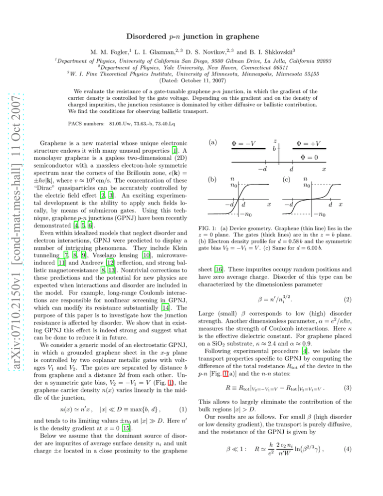
We consider a generic model of an electrostatic GPNJ,
in which a grounded graphene sheet in the x-y plane
is controlled by two coplanar metallic gates with voltages V1 and V2 . The gates are separated by distance b
from graphene and a distance 2d from each other. Under a symmetric gate bias, V2 = −V1 = V (Fig. 1), the
graphene carrier density n(x) varies linearly in the middle of the junction,
n(x) ≃ n′ x ,
|x| ≪ D ≡ max{b, d} ,
(1)
and tends to its limiting values ±n0 at |x| ≫ D. Here n′
is the density gradient at x = 0 [15].
Below we assume that the dominant source of disorder are impurites of average surface density ni and unit
charge ±e located in a close proximity to the graphene
(a)
z
b
Φ = −V
Φ = +V
Φ=0
(b)
−d
n
n0
−d
(c)
x
d
−n0
x
d
−d
n
n0
d x
−n0
FIG. 1: (a) Device geometry. Graphene (thin line) lies in the
z = 0 plane. The gates (thick lines) are in the z = b plane.
(b) Electron density profile for d = 0.58 b and the symmetric
gate bias V2 = −V1 = V . (c) Same for d = 6.00 b.
sheet [16]. These impurites occupy random positions and
have zero average charge. Disorder of this type can be
characterized by the dimensionless parameter
3/2
β = n′ /ni .
(2)
Large (small) β corresponds to low (high) disorder
strength. Another dimensionless parameter, α = e2 /κ~v,
measures the strength of Coulomb interactions. Here κ
is the effective dielectric constant. For graphene placed
on a SiO2 substrate, κ ≈ 2.4 and α ≈ 0.9.
Following experimental procedure [4], we isolate the
transport properties specific to GPNJ by computing the
difference of the total resistance Rtot of the device in the
p-n [Fig. 1(a)] and the n-n states:
R ≡ Rtot |V2 =−V1 =V − Rtot |V2 =V1 =V .
(3)
This allows to largely eliminate the contribution of the
bulk regions |x| > D.
Our results are as follows. For small β (high disorder
or low density gradient), the transport is purely diffusive,
and the resistance of the GPNJ is given by
β≪1:
R≃
h 2 c2 n i
ln β 2/3 γ ,
e 2 n′ W
(4)
2
where W is the length of the device in the y-direction,
the coefficient c2 is discussed below, and γ is defined by
γ ≡ (n′ )1/3 D ≫ 1 .
(5)
The condition γ ≫ 1, which is satisfied in experiment [4, 5, 6], ensures that the density n(x) varies across
the GPNJ slowly enough, D = max{d, b} ≫ kF−1 (n0 ),
to justify its evaluation by
pmeans of classical electrostatics [14]. Here kF (n) = π|n| is the local Fermi wave
vector. Equation (4) is written for β 2/3 γ ≫ 1, i.e., for
n0 ≫ ni , where the GPNJ is still well-defined despite
random fluctuations of the electron density n(x, y) due
to disorder.
In the opposite regime, β ≫ 1, the GPNJ resistance
β≫1 :
R = Rbal + Rdif
(6a)
is the sum of the ballistic and the diffusive contributions,
c1
h
, c1 ≈ 1.0 ;
e2 α1/6 (n′ )1/3 W
γ
h 2 c2 n i
ln 4/3 , γ ≫ β 4/3 .
≃ 2 ′
e nW
β
Rbal =
(6b)
Rdif
(6c)
Equations (4) and (6c) are valid with logarithmic accuracy and match at β ∼ 1. The ballistic contribution
dominates, R ≃ Rbal ≫ Rdif , provided
β≫
2α1/6 c2
ln
c1
γ
β 4/3
3/2
.
(7)
Realistically, the “large” logarithmic factor here is ∼ 2.
Thus the right-hand side of Eq. (7) is about 0.3–0.5. In
comparison, we estimate for recent experiments [4, 6] β ∼
0.5. This puts them in the crossover regime where Rbal ∼
Rdif . (The reported data suggests Rbal W ∼ Rdif W ∼
1 Ω · cm). To move deeper into the ballistic regime one
should either increase n′ or decrease ni .
Below we first consider electrostatics of the gatetunable junction, and then evaluate its resistance.
Electrostatics.— Electron density in graphene is related to the electrostatic potential Φ(x, z) by the Gauss
law, n(x) = (κ/4π)∂z Φ(x, +0). To find Φ and n we can
treat graphene as an ideal conductor. (For the discussion of this approximation, see Refs. [14] and [17].) The
calculation can be done using the conformal mapping
π
a+w
(8)
= (x + iz) ,
2w + ln
a−w
b
which transforms the upper half-plane z > 0 with the
branch cuts along the gates [cf. Fig. 1(a)] to the upper
half-plane of a complex variable w = w(x, z). Here a is
found from
p
√
√
a(a + 1) + ln( a + a + 1 ) = πd/(2b) .
(9)
The graphene sheet, the left gate, and the right gate
are mapped onto the intervals −a < w < a, w < −a,
and w > a, respectively, of the real axis. Therefore, the
sought potential is given by
Φ(x, z) = (1/π) Im [V1 ln(a + w) − V2 ln(a − w)] . (10)
Using these equations and simple algebra, we find
n(x) =
κ (V2 + V1 )a + (V2 − V1 )w(x)
,
8πb
a(a + 1) − w2 (x)
(11)
where w(x) stands for the real quantity w(x, z = 0) defined by Eq. (8). For the symmetric gate bias we obtain
n0 (V )w(x)
,
a(a + 1) − w2 (x)
n(x) =
V2 = −V1 = V ,
(12)
in which case the density gradient at x = 0 is given by
n′ =
π n0 (V )
,
2b (1 + a)2
n0 (V ) =
κV
.
4πb
(13)
Examples of n(x) computed according to Eqs. (8) and
(12) are plotted in Fig. 1(b) and (c).
Ballistic resistance.— The resistance Rbal of a clean
GPNJ is related [8] to the electric field at the p-n
interface. To compute this field one has to go beyond electrostatics of ideal conductors and take into account nonlinear screening at the p-n interface. Equation (6b) for Rbal was derived from this analysis in
Ref. [14]. A simple explanation of this result can be
given in the case α ∼ 1, where Rbal can be qualitatively understood as the
ballistic resistance of a system with W kF n(xtun ) transmitting channels: Rbal ∼
(h/e2 )(kF W )−1 ∼ (h/e2 )(xtun /W ). Here the effective
“width” of the p-n interface
xtun = α−1/6 (n′ )−1/3
(14)
is found from the condition that it is of the order of
the quantum uncertainty
in the quasiparticle coordinate,
xtun ∼ kF−1 n(xtun ) . (In Ref. [14] xtun was denoted by
xTF .) The quasiparticles that manage to get inside the
strip |x| < xtun cross the p-n boundary without tunneling
suppression [8].
Below we consider the resistance (3) of a symmetrically
biased GPNJ, V2 = −V1 = V . The transport is either
diffusive or ballistic depending on the gradient (2).
Diffusive transport, β ≪ 1.— Introduction of charged
impurities results in the finite carrier mean free path
l(n) = 1/ni Λ ,
Λ = 2πc2 (α)/kF (n) ,
(15)
where Λ is the transport cross-section for Coulomb impurities [18, 19, 20, 21]. For α ≪ 1 (graphene on large-κ
substrate), c2 = πα2 /2, while for α ≈ 1 (SiO2 substrate),
c2 ∼ 0.1 [22]. Impurities act as independent scatterers if
|n| ≫ ni . The corresponding resistivity is [18, 19, 20, 21]
ρ(n) =
h ni
h
= 2
c2 (α) ,
2e2 kF l
e |n|
|n| ≫ ni .
(16)
3
(a)
x
0
x tun x flc
x flc
D
x bal
x
(b)
0 x tun
D
FIG. 2: A sketch of the characteristic lengthscales in a GPNJ
for (a) β ≪ 1 and (b) β ≫ 1. Only the x > 0 side of the junction is shown. The diffusive region is hatched. Parameters
xtun and xflc are indicated by the dashed lines in the regimes
(a) and (b), respectively, because they do not have a direct
physical meaning in these cases.
It is legitimate to treat ρ n(x) as the local x-dependent
resistivity if the density gradient is sufficiently small, such
that l(n)|∂x n| ≪ n. For β ≪ 1 this condition is satisfied
at all |x| ≫ ni /n′ where Eq. (16) is itself valid, |n| ≫
ni . On the other hand, in the strip |x| . xflc = ni /n′
[Fig. 2(a)], the disorder-induced fluctuations of the local
density overwhelm the average n(x) ≃ n′ x dependence.
As a result, Eq. (16) no longer holds.
Since the transport remains diffusive in this strip (certainly, it cannot be ballistic because of strong disorder) [23], we can assume that the corresponding local
resistivity is of the order of its bulk value ρ ∼ h/e2 at
the charge neutrality point [3]. This allows us to estimate
the resistance of this region as ∼ (h/e2 )(xflc /W ).
According to our definition (3), the GPNJ resistance is
the difference of the total resistances in the p-n and n-n
configurations. It is convenient to write it as R = Rdif (0),
where
Z∞
2
dx̃ ρ(x̃)|V1 =−V2 − ρ(x̃)|V1 =+V2 . (17)
Rdif (x) =
W
x
Using Eqs. (8), (12), (16), and the expression
n(x) =
n0 (V )a
,
a(a + 1) − w2 (x)
V1 = V2 = V ,
(18)
for the charge profile in the n-n state that follows from
Eq. (11), the integral in Eq. (17) can be transformed to
n0
h 2c2 ni
, x & xflc . (19)
ln
Rdif (x) ≃ 2 ′
e nW
(a + 1)n′ x
This resistance is logarithmically larger than
(h/e2 )(xflc /W ).
In other words, the resistance of
the |x| < xflc strip is much smaller than that of the rest
of the junction. Therefore, R ≃ Rdif (xflc ), which leads
to Eq. (4).
Ballistic transport, β ≫ 1.— Here the carrier density
n(x) varies with x more rapidly. As a result, the diffusive
approximation breaks down inside the strip |x| . xbal
whose width is given by the condition l[n(xbal )] ∼ xbal ,
xbal ∼
1 n′
.
4πc22 n2i
(20)
The carrier density at x = xbal is still high, n(xbal ) ≫ ni ,
so that at |x| > xbal Eq. (16) applies. Thus, the diffusive contribution to the resistance is Rdif ≃ Rdif (xbal ),
leading to Eq. (6c). [The extra factor β −2 under the
logarithm in Eq. (6c) vs. (4) comes from xbal ∼ β 2 xflc .
Note, however, that xflc has no direct physical meaning
if β ≫ 1.]
In contrast, within the strip |x| < xbal the transport is
ballistic: the local mean-free path l[n(x)] nominally exceeds |x|, so that quasiparticles reach the p-n interface
largely without experiencing impurity scattering. We
now note that the tunneling strip (20) is located deep
inside this ballistic region,
xtun ∼
4πc22 xbal
≪ xbal ,
α1/6 β 4/3
(21)
see Fig. 2(b). Therefore, the transmission problem is
reduced to the clean case [14], yielding Eq. (6b) for the
ballistic resistance Rbal .
Due to the large logarithmic factor in Rdif [Eq. (6c)],
the ballistic contribution in Eq. (6a) starts to dominate
the diffusive one only when β exceeds a logarithmically
large threshold, Eq. (7). In other words, the ballistic
transport is observable only for a GPNJ with a sufficiently large concentration gradient.
Let us illustrate geometrical requirements imposed by
the criterion (7) assuming α ∼ 1. Consider first the case
of widely separated gates, d = 1 µm and b = 50 nm. For
the impurity concentration ni ∼ 1012 cm−2 (presumed
to be a typical number), we get β ≈ 0.005 even for a
relatively high maximum density n0 ∼ 10ni ∼ 1013 cm−2 .
Thus, in this kind of a GPNJ one cannot observe ballistic
transport. On the other hand, in a shorter device, b ≈
d ≈ 40 nm, such as that of Ref. [4], the minimum density
needed to reach the ballistic regime, β ∼ 0.5, is close to
the experimental value n0 = 2 × 1012 cm−2 [4] at which
evidence of the ballistic resistance was indeed seen.
To conclude, the presence of charged disorder results
in the two distinct transport regimes in the junction.
The GPNJ resistance in the ballistic regime is given by
Eqs. (6), and in the diffusive regime by Eq. (4). In the
current experiments [4, 5, 6], the ballistic regime was
reached only marginally. For ballistic devices one should
aim at larger electron density gradients n′ and smaller
impurity concentration to satisfy the condition (7). The
requirement on n′ becomes less stringent for substrates
of high dielectric constant κ, which reduces the weight
c2 ∝ α2 ∝ κ−2 of Coulomb scattering. Finally, the
present approach can be extended to other geometries
that involve local gate control of graphene nanostructures
(asymmetric junctions, multiple gates, etc.).
This work is supported by the Grants NSF DMR0706654 (M. F.) and NSF DMR-0749220 (L. G., D. N.).
M. F. thanks the W. I. Fine TPI for hospitality.
4
[1] A. K. Geim and K. S. Novoselov, Nature Mater. 6, 183
(2007); A. H. Castro Neto, F. Guinea, N. M. R. Peres,
K. S. Novoselov, and A. K. Geim, arXiv:0709.1163
(2007).
[2] K. S. Novoselov, A. K. Geim, S. V. Morozov, D. Jiang,
Y. Zhang, S. V. Dubonos, I. V. Grigorieva, and A. A.
Firsov, Science 306, 666 (2004).
[3] K. S. Novoselov, A. K. Geim, S. V. Morozov, D. Jiang,
M. I. Katsnelson, I. V. Grigorieva, S. V. Dubonos, and
A. A. Firsov, Nature 438, 197 (2005).
[4] B. Huard, J. A. Sulpizio, N. Stander, K. Todd, B. Yang,
and D. Goldhaber-Gordon, Phys. Rev. Lett. 98, 236803
(2007).
[5] B. Özyilmaz, P. Jarillo-Herrero, D. Efetov, D. A. Abanin,
L. S. Levitov, and P. Kim, arXiv:0705.3044 (2007).
[6] J. R. Williams, L. DiCarlo, and C. M. Marcus, Science
317, 638 (2007).
[7] M. I. Katsnelson, K. S. Novoselov, and A. K. Geim, Nature Phys. 2, 620 (2006).
[8] V. V. Cheianov and V. I. Fal’ko, Phys. Rev. B 74, 041403
(2006).
[9] J. M. Pereira, Jr., V. Mlinar, F. M. Peeters, and
P. Vasilopoulos, Phys. Rev. B 74, 045424 (2006).
[10] V. V. Cheianov, V. I. Fal’ko, and B. L. Altshuler, Science
315, 1252 (2007).
[11] M. V. Fistul and K. B. Efetov, Phys. Rev. Lett. 98,
256803 (2007).
[12] A. Ossipov, M. Titov, and C. W. J. Beenakker, Phys.
Rev. B 75, 241401(R) (2007).
[13] A. V. Shytov, N. Gu, and L. S. Levitov, arXiv:0708.3081
(2007).
[14] L. M. Zhang and M. M. Fogler, arXiv:0708.0892 (2007).
[15] Note that n′ stands for the density gradient computed
classically. Quantum effects decrease true n′ [14].
[16] J. H. Chen, C. Jang, M. S. Fuhrer, E. D. Williams, and
M. Ishigami, arXiv:0708.2408 (2007).
[17] See M. M. Fogler, D. S. Novikov, and B. I. Shklovskii,
arXiv:0707.1023 (2007) and references therein.
[18] T. Ando, J. Phys. Soc. Jpn. 75, 074716 (2006).
[19] K. Nomura and A. H. MacDonald, Phys. Rev. Lett. 98,
076602 (2007).
[20] E. H. Hwang, S. Adam, and S. Das Sarma, Phys. Rev.
Lett. 98, 186806 (2007).
[21] D. S. Novikov, arXiv:0706.1391 (2007); Appl. Phys. Lett.
91, 102102 (2007).
[22] Treating the impurity screening within the Random
Phase Approximation (RPA) and calculating the scattering cross-section perturbatively yields c2 (0.9) ≈ 0.05
[18, 20]. For α ∼ 1 this calculation is likely to underestimate c2 . Using the RPA at the Dirac point and treating scattering off the resultant Coulomb potential exactly
yields c2 (0.9) ≈ 0.26 (when averaged over the donors and
acceptors) [21]. This is likely to overestimate the resistivity. Thus, the true c2 (α ∼ 1) is probably close to 0.1.
[23] In addition, we assume that the temperature is not too
low and neglect any localization effects.


