DIGITAL TO ANALOG CONVERTERS
advertisement
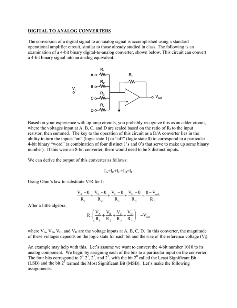
DIGITAL TO ANALOG CONVERTERS The conversion of a digital signal to an analog signal is accomplished using a standard operational amplifier circuit, similar to those already studied in class. The following is an examination of a 4-bit binary digital-to-analog converter, shown below. This circuit can convert a 4-bit binary signal into an analog equivalent. R1 Rf A R2 Vi B R3 C R4 Vout + D Based on your experience with op-amp circuits, you probably recognize this as an adder circuit, where the voltages input at A, B, C, and D are scaled based on the ratio of Rf to the input resistor, then summed. The key to the operation of this circuit as a D/A converter lies in the ability to turn the inputs “on” (logic state 1) or “off” (logic state 0) to correspond to a particular 4-bit binary “word” (a combination of four distinct 1’s and 0’s that serve to make up some binary number). If this were an 8-bit converter, there would need to be 8 distinct inputs. We can derive the output of this converter as follows: IA+IB+IC+ID=IF Using Ohm’s law to substitute V/R for I: VA − 0 VB − 0 VC − 0 VD − 0 0 − Vout + + + = R1 R2 R3 R4 Rf After a little algebra: ⎛V V V V ⎞ R f ⎜⎜ A + B + C + D ⎟⎟ = −Vout ⎝ R1 R 2 R 3 R 4 ⎠ where VA, VB, VC, and VD are the voltage inputs at A, B, C, D. In this converter, the magnitude of these voltages depends on the logic state for each bit and the size of the reference voltage (Vi). An example may help with this. Let’s assume we want to convert the 4-bit number 1010 to its analog component. We begin by assigning each of the bits to a particular input on the converter. The four bits correspond to 20, 21, 22, and 23, with the bit 20 called the Least Significant Bit (LSB) and the bit 23 termed the Most Significant Bit (MSB). Let’s make the following assignments: Binary Value 0001 (LSB) 0010 0100 1000 (MSB) Input A B C D Analog Equivalent 20 = 1 21 = 2 22 = 4 23 = 8 So, for our digital 1010, the converter would apply Vi, which is typically +5 volts, to inputs B and D, while leaving A and C at 0 V, and the output of the converter would be: R1 Rf A R2 +5V B - R3 C R4 Vout + D ⎛ 0 V + 5V 0 V + 5V ⎞ ⎟⎟ = − Vout R f ⎜⎜ + + + R R R R 2 3 4 ⎠ ⎝ 1 In order to make a prediction of the actual voltage output, we need to assign vales to the resistors in the circuit. In principle, most any resistance would work, but a little consideration of utility makes some choices better than others. Another look at the table above suggests that the word 0010 should output a voltage twice the size of 0001, while 0100 should be four times the size of 0001 and 1000 eight times the size. Therefore, it is useful to design the circuit to give this 1:2:4:8 scaling of the reference voltage. In order to accomplish this, the resistors for larger bits must have a smaller resistance (or larger weighting). More importantly, the resistance must decrease by the 1:2:4:8 ratio. The following pattern emerges: R2 = R1/2, R3 = R1/4, and R4 = R1/8. Under these conditions, the output function of the system becomes: ⎛V V V V ⎞ R f ⎜⎜ A + B + C + D ⎟⎟ = −Vout ⎝ R1 R1 2 R1 4 R1 8 ⎠ After some more algebra, we get a final relationship: Rf (VA + 2VB + 4VC + 8VD ) = −Vout R1 Remember VA – VD are either 0V or +5V (Vi), depending on the whether the bit is on (1) or off (0). The magnitudes of Rf and R1 are fairly arbitrary, but are often chosen so that Rf/R1 = 1/Vi so that the analog output mirrors the digital inputs. Let’s now apply this to the following figure, where R1 = 40 KΩ and Rf= 8 KΩ (Rf/R1 =1/5) . By following the logic above, R2 must be ½ that of R1, meaning it must be a 20 KΩ resistor; R3 is a 10 KΩ resistor and R4 is a 5 KΩ resistor. 40 kΩ A 8 kΩ 20 kΩ Vi B 10 kΩ C 5 kΩ + D Our derived relationship becomes 8 (VA + 2VB + 4VC + 8VD ) = −Vout 40 Just what the heck does this mean? Let’s put some digital numbers into the circuit and find out. How about the binary equivalent of 10, which is 1010 in binary notation? 4-bit binary number 1 0 1 0 Position of binary signal at op-amp input D C B A Corresponding input voltage VD =+5V VC = 0V VB = +5V VA = 0V Plug in to the relation 8 (VA + 2VB + 4VC + 8VD ) = −Vout 40 8 (0V + 2(5V ) + 0V + 8(5V )) = −Vout 40 1 (50V ) = 10V = −Vout 5 How ‘bout that. 10V digital = 10V analog We can also determine the size of the least significant bit (0001). If a numerical 1 is placed in the LSB, then the outcome is 8 (5V + 0 + 0 + 0) = −Vout 40 1 (5V ) = 1V = −Vout 5 In this 4-bit DAC, the resolution of this device is 24=16 or 1 part in 16. (e.g. 16 different output voltages, ranging from 0 to 15v, in 1 volt increments). One last question: Why, if the weighing of digits in a binary number is 8:4:2:1, is the input resistor ladder opposite that you might expect? A, the LSB has the largest resistor (8x that of the MSB input).
