Document Number: MPL115A1
Rev. 7, 02/2013
Freescale Semiconductor
Data Sheet: Technical Data
Miniature SPI Digital Barometer
MPL115A1
The MPL115A1 is an absolute pressure sensor with a digital SPI output targeting
low cost applications. A miniature 5 x 3 x 1.2 mm LGA package is ideally suited
for the space constrained requirements of portable electronic devices. Low
current consumptions of 5 μA during Active mode and 1 μA during Shutdown
(Sleep) mode are essential when focusing on low-power applications. The wide
operating temperature range spans from -40°C to +105°C to fit demanding
environment conditions.
50 to 115 kPa
The MPL115A1 employs a MEMS pressure sensor with a conditioning IC to
provide accurate pressure measurements from 50 to 115 kPa. An integrated
ADC converts pressure and temperature sensor readings to digitized outputs via
a SPI port. Factory calibration data is stored internally in an on-board ROM.
Utilizing the raw sensor output and calibration data, the host microcontroller
executes a compensation algorithm to render Compensated Absolute Pressure
with ±1 kPa accuracy.
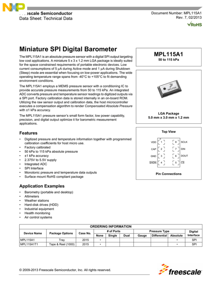
LGA Package
5.0 mm x 3.0 mm x 1.2 mm
The MPL115A1 pressure sensor’s small form factor, low power capability,
precision, and digital output optimize it for barometric measurement
applications.
Top View
Features
•
•
•
•
•
•
•
•
•
Digitized pressure and temperature information together with programmed
calibration coefficients for host micro use.
Factory calibrated
50 kPa to 115 kPa absolute pressure
±1 kPa accuracy
2.375V to 5.5V supply
Integrated ADC
SPI Interface
Monotonic pressure and temperature data outputs
Surface mount RoHS compliant package
VDD
1
8
SCLK
CAP
2
7
DIN
GND
3
6
DOUT
SHDN
4
5
CS
Pin Connections
Application Examples
•
•
•
•
•
•
•
Barometry (portable and desktop)
Altimeters
Weather stations
Hard-disk drives (HDD)
Industrial equipment
Health monitoring
Air control systems
ORDERING INFORMATION
Device Name
MPL115A1
MPL115A1T1
Package Options
Case No.
Tray
2015
Tape & Reel (1000)
2015
# of Ports
Pressure Type
Absolute
Digital
Interface
•
•
SPI
•
•
SPI
None
Single
© 2009-2013 Freescale Semiconductor, Inc. All rights reserved.
Dual
Gauge
Differential
1
Block Diagram and Pin Descriptions
1 μF
VDD
VDD
ADDR
Coefficient
Storage
ADDR
CAP
CAP
1 μF
ADDR
Diff
Amp
MUX
SHDN
ADC
ADDR
Pressure
ADDR
Temperature
Temp
Sensor
SHDN
SCLK
SCLK
DIN
SPI
Interface
DIN
μC
Microcontroller
DOUT
DOUT
CS
CS
GND
GND
Figure 1. Block Diagram and Pin Connections
Table 1. Pin Description
Pin
Name
Function
1
VDD
VDD Power Supply Connection: VDD range is 2.375V to 5.5V.
2
CAP
External Capacitor: Output decoupling capacitor for main internal regulator. Connect a 1 μF ceramic capacitor
to ground.
3
GND
Ground
4
SHDN
5
CS
6
DOUT
7
DIN
8
SCLK
Shutdown: Connect to GND to disable the device. When in shut down the part draws no more than 1 μA supply
current and all communications pins (CS, SCLK, DOUT, DIN) are high impedance. Connect to VDD for normal
operation.
CS: Chip Select line.
DOUT: Serial data output
DIN: Serial data input
SPI: Serial Clock Input.
MPL115A1
2
Sensors
Freescale Semiconductor, Inc.
2
Mechanical and Electrical Specifications
2.1
Maximum Ratings
Voltage (with respect to GND unless otherwise noted)
VDD ..................................................................................................................... -0.3 V to +5.5 V
SHDN, SCLK, CS, DIN, DOUT ......................................................................-0.3 V to VDD+0.3 V
Operating Temperature Range .......................................................................... -40°C to +105°C
Storage Temperature Range ............................................................................. -40°C to +125°C
Overpressure................................................................................................................ 1000 kPa
2.2
Operating Characteristics
(VDD = 2.375 V to 5.5 V, TA = -40°C to +105°C, unless otherwise noted. Typical values are at VDD = 3.3 V, TA = +25°C.
Ref
Parameters
Symbol
1
Operating Supply Voltage
VDD
2
Supply Current
IDD
Conditions
Min
Typ
Max
Units
2.375
3.3
5.5
V
Shutdown (SHDN = GND)
—
—
1
μA
Standby
—
3.5
10
μA
Average – at one measurement per second
—
5
—
μA
Pressure Sensor
3
Range
50
—
115
kPa
4
Resolution
—
0.15
—
kPa
5
Accuracy
-20ºC to 85ºC
—
—
±1
kPa
6
Conversion Time
(Start Pressure and Temperature
Conversion)
tc
Time between start convert command and
data available in the Pressure and
Temperature registers
—
1.6
3
ms
7
Wakeup Time
tw
Time between leaving Shutdown mode
(SHDN goes high) and communicating with
the device to issue a command or read data.
—
3
5
ms
(1)
—
—
8
MHz
SPI Inputs: SCLK, CS, DIN
8
SCLK Clock Frequency
fSCLK
9
Low Level Input Voltage
VIL
—
—
0.3VDD
V
10
High Level Input Voltage
VIH
0.7VDD
—
—
V
V
SPI Outputs: DOUT
11
12
Low Level Output Voltage
High Level Output Voltage
VOL1
At 3 mA sink current
0
—
0.4
VOL2
At 6 mA sink current
0
—
0.6
VDD – 0.4 V
—
—
VOH1 At 3 mA source current
V
1.Nominal maximum SPI clock frequency.
MPL115A1
Sensors
Freescale Semiconductor, Inc.
3
3
Overview of Functions/Operation
Initial
powerup
Reading
coefficient data
Data conversion
Compensated
pressure reading
Shutdown
Figure 2. Sequence Flow Chart
The MPL115A interfaces to a host (or system) microcontroller in the user’s application. All communications are via SPI. A typical
usage sequence is as follows:
Initial Power-up
All circuit elements are active. SPI port pins are high impedance and associated registers are cleared. The device then enters
standby mode.
Reading Coefficient Data
The user then typically accesses the part and reads the coefficient data. The main circuits within the slave device are disabled
during read activity. The coefficients are usually stored in the host microcontoller local memory but can be re-read at any time.
Reading of the coefficients may be executed only once and the values stored in the host microcontroller. It is not necessary to
read this multiple times because the coefficients within a device are constant and do not change. However, note that the
coefficients will be different from device to device, and cannot be used for another part.
Data Conversion
This is the first step that is performed each time a new pressure reading is required which is initiated by the host sending the
CONVERT command. The main system circuits are activated (wake) in response to the command and after the conversion
completes, the result is placed into the Pressure and Temperature ADC output registers.
The conversion completes within the maximum conversion time, tc (see Row 6, in the Operating Characteristics Table). The
device then enters standby mode.
Compensated Pressure Reading
After the conversion has been given sufficient time to complete, the host microcontroller reads the result from the ADC output
registers and calculates the Compensated Pressure, a barometric/atmospheric pressure value which is compensated for
changes in temperature and pressure sensor linearity. This is done using the coefficient data from the MPL115A and the raw
sampled pressure and temperature ADC output values, in a compensation equation (detailed later). Note that this is an absolute
pressure measurement with a vacuum as a reference.
From this step the host controller may either wait and then return to the Data Conversion step to obtain the next pressure reading
or it may go to the Shutdown step.
MPL115A1
4
Sensors
Freescale Semiconductor, Inc.
Shutdown
For longer periods of inactivity the user may assert the SHDN input by driving this pin low to reduce system power consumption.
This removes power from all internal circuits, including any registers. In the shutdown state, the Pressure and Temperature
registers will be reset, losing any previous ADC output values.
This step is exited by taking the SHDN pin high. Wait for the maximum wakeup time, tw (see Row 7, in the Operating
Characteristics Table), after which another pressure reading can be taken by transitioning to the data Conversion step.
Table 2. Device Memory Map
Address
Name
Description
0x00
Padc_MSB
10-bit Pressure ADC output value MSB
0x01
Padc_LSB
10-bit Pressure ADC output value LSB
0x02
Tadc_MSB
10-bit Temperature ADC output value MSB
0x03
Tacd_LSB
10-bit Temperature ADC output value LSB
0x04
a0_MSB
a0 coefficient MSB
0x05
a0_LSB
a0 coefficient LSB
0x06
b1_MSB
b1 coefficient MSB
0x07
b1_LSB
b1 coefficient LSB
0x08
b2_MSB
b2 coefficient MSB
0x09
b2_LSB
b2 coefficient LSB
0x0A
c12_MSB
c12 coefficient MSB
0x0B
c12_LSB
c12 coefficient LSB
0x0C
Reserved*
—
0x0D
Reserved*
—
0x0E
Reserved*
—
0x0F
Reserved*
—
0x10
Reserved
—
0x11
Reserved
—
0x12
CONVERT
Start Pressure and Temperature Conversion
*These registers are set to 0x00. These are reserved, and were previously utilized as Coefficient values, c11 and c22, which
were always 0x00.
For values with less than 16 bits, the lower LSBs are zero. For example, c12 is 14 bits and is stored into 2 bytes as follows:
c12 MS byte = c12[13:6] = [c12b13 , c12b12 , c12b11 , c12b10 , c12b9 , c12b8 , c12b7 , c12b6]
c12 LS byte = c12[5:0] & “00” = [c12b5 , c12b4 , c12b3 , c12b2 , c12b1 , c12b0 , 0 , 0]
3.1
Pressure, Temperature and Coefficient Bit-Width Specifications
The table below specifies the initial coefficient bit-width specifications for the compensation algorithm and the specifications for
Pressure and Temperature ADC values.
Pressure, Temperature and Compensation Coefficient Specifications
a0
b1
b2
c12
Padc
Tadc
Total Bits
16
16
16
14
10
10
Sign Bits
1
1
1
1
0
0
Integer Bits
12
2
1
0
10
10
Fractional Bits
3
13
14
13
0
0
dec pt zero pad
0
0
0
9
0
0
MPL115A1
Sensors
Freescale Semiconductor, Inc.
5
Example Binary Format Definitions:
a0 Signed, Integer Bits = 12, Fractional Bits = 3 :
Coeff a0 = S I11 I10 I9 I8 I7 I6 I5 I4 I3 I2 I1 I0 . F2 F1 F0
b1 Signed, Integer Bits = 2, Fractional Bits = 13 :
Coeff b1 = S I1 I0 . F12 F11 F10 F9 F8 F7 F6 F5 F4 F3 F2 F1 F0
b2 Signed, Integer Bits = 1, Fractional Bits = 14 :
Coeff b2 = S I0 . F13 F12 F11 F10 F9 F8 F7 F6 F5 F4 F3 F2 F1 F0
c12 Signed, Integer Bits = 0, Fractional Bits = 13, dec pt zero pad = 9 :
Coeff c12 = S 0 . 000 000 000 F12 F11 F10 F9 F8 F7 F6 F5 F4 F3 F2 F1 F0
Padc Unsigned, Integer Bits = 10 :
Padc U = I9 I8 I7 I6 I5 I4 I3 I2 I1 I0
Tadc Unsigned, Integer Bits =10 :
Tadc U = I9 I8 I7 I6 I5 I4 I3 I2 I1 I0
NOTE: Negative coefficients are coded in 2’s complement notation.
3.2
Compensation
The 10-bit compensated pressure output, Pcomp, is calculated as follows:
Pcomp = a0 + ( b1 + c12 ⋅ Tadc ) ⋅ Padc + b2 ⋅ Tadc
Eqn. 1
Where:
Padc is the 10-bit pressure ADC output of the MPL115A
Tadc is the 10-bit temperature ADC output of the MPL115A
a0 is the pressure offset coefficient
b1 is the pressure sensitivity coefficient
b2 is the temperature coefficient of offset (TCO)
c12 is the temperature coefficient of sensitivity (TCS)
Pcomp will produce a value of 0 with an input pressure of 50 kPa and will produce a full-scale value of 1023 with an input pressure
of 115 kPa.
Pressure (kPa) = P comp
3.3
⋅
115 – 50
---------------------- + 50
1023
Eqn. 2
Evaluation Sequence, Arithmetic Circuits
The following is an example of the calculation for Pcomp, the compensated pressure output. Input values are in bold.
c12x2 = c12 * Tadc
a1 = b1 + c12x2
a1x1 = a1 * Padc
y1 = a0 + a1x1
a2x2 = b2 * Tadc
Pcomp = y1 + a2x2
This can be calculated as a succession of Multiply Accumulates (MACs) operations of the form y = a + b * x:
a
b
+
y
X
x
MPL115A1
6
Sensors
Freescale Semiconductor, Inc.
The polynomial can be evaluated (Equation 1) as a sequence of 3 MACs:
Pcomp = a0 + ( b1 + c12 ⋅ Tadc ) ⋅ Padc + b2 ⋅ Tadc
b1
a1
c12
Tadc
y1
a0
Padc
y
b2
PComp
Tadc
Please refer to Freescale application note AN3785 for more detailed notes on implementation.
3.4
SPI Device Read/Write Operations
All device read/write operations are memory mapped. Device actions e.g. “Start Conversions” are controlled by writing to the
appropriate memory address location. All memory address locations are 6-bit (see Table 2).
The 8-bit command word comprises:
• the most significant bit which is the Read/Write identifier which is '1' for read operations and '0' for write operations.
• the 6-bit address (from Table 2);
• the least significant bit which is not used and is don't care (X).
The device write commands are shown in Table 3.
Table 3. SPI Write Command
Command
Start Conversions
Binary
HEX(1)
0010010X
0x24
X = don’t care
1. The command byte needs to be paired with a 0x00 as part of the SPI exchange to complete the passing of Start
Conversions.
The actions taken by the part in response to each command are as follows:
Table 4. SPI Write Command Description
Command
Start Conversions
Action Taken
Wake main circuits. Start clock. Allow supply stabilization time. Select pressure sensor input.
Apply positive sensor excitation and perform A to D conversion. Select temperature input.
Perform A to D conversion. Load the Pressure and Temperature registers with the result. Shut
down main circuits and clock.
MPL115A1
Sensors
Freescale Semiconductor, Inc.
7
SPI Read operations are performed by sending the required address with a leading Read bit set to ‘1’. SPI operations require
that each byte be addressed individually. All data is transmitted most significant bit first.
Table 5. Example SPI Read Commands
Binary
HEX(1)
Read Pressure MSB
1000000X
0x80
Read Pressure LSB
1000001X
0x82
Read Temperature MSB
1000010X
0x84
Read Temperature LSB
1000011X
0x86
Read Coefficient data byte 1
1000100X
0x88
Command
X = don’t care
1. The command byte needs to be paired with a 0x00 as part of the SPI exchange to complete the passing of stated
command.
3.5
SPI Timing
Table 6 and Figure 3 describe the timing requirements for the SPI system.
Table 6. SPI Timing
Ref
Function
Symbol
Min
Max
Unit
Of
—
8
MHz
1
Operating Frequency
2
SCLK Period
tSCLK
125
—
ns
3
SCLK High time
tCLKH
62.5
—
ns
4
SCLK Low time
tCLKL
62.5
—
ns
5
Enable lead time
tSCS
125
—
ns
6
Enable lag time
tHCS
125
—
ns
7
Data setup time
tSET
30
—
ns
8
Data hold time
tHOLD
30
—
ns
9
Data valid (after SCLK low edge)
tDDLY
—
32
ns
10
Width CS High
tWCS
30
—
ns
CS
SCLK
DIN
DOUT
Figure 3. SPI Timing Diagram
MPL115A1
8
Sensors
Freescale Semiconductor, Inc.
3.6
Example of SPI Reading of Coefficients
These are MPL115A1 SPI commands to read coefficients, execute Pressure and Temperature conversions, and to read Pressure
and Temperature data. The sequence of the commands for the interaction is given as an example to operate the MPL115A1.
Utilizing this gathered data, an example of the calculating the Compensated Pressure reading is given in floating point notation.
SPI Commands (simplified for communication)
Command to Write “Convert Pressure and Temperature” = 0x24
Command to Read “Pressure ADC High byte” = 0x80
Command to Read “Pressure ADC Low byte” = 0x82
Command to Read “Temperature ADC High byte” = 0x84
Command to Read “Temperature ADC Low byte” = 0x86
Command to Read “Coefficient data byte 1 High byte” = 0x88
Read Coefficients:
[CS=0], [0x88], [0x00], [0x8A], [0x00], [0x8C], [0x00], [0x8E], [0x00], [0x90], [0x00], [0x92], [0x00], [0x94], [0x00], [0x96], [0x00],
[0x00], [CS=1]
Start Pressure and Temperature Conversion, Read raw Pressure:
[CS=0], [0x24], [0x00], [CS=1], [3 ms Delay]
[CS=0], [0x80], [0x00], [0x82], [0x00], [0x84], [0x00,] [0x86], [0x00], [0x00], [CS=1]
NOTE: Extra [0x00] at the end of each sequence to output the last data byte on the slave side of the SPI.
Figure 4. SPI Read Coefficient Datagram
a0 coefficient MSB
= 0x41
a0 coefficient LSB
= 0xDF a0 coefficient
b1 coefficient MSB
= 0xB0
b1 coefficient LSB
= 0x28
b2 coefficient MSB
= 0xBE
b2 coefficient LSB
= 0xAD b2 coefficient
b1 coefficient
= 0x41DF
= 2107.875
= 0xB028
= -2.49512
= 0xBEAD =
-1.02069
c12 coefficient MSB = 0x38
c12 coefficient LSB
= 0xCC c12 coefficient = 0x38CC = 0.00086665
MPL115A1
Sensors
Freescale Semiconductor, Inc.
9
Figure 5. SPI Start Conversion Datagram
Command to Start Pressure and Temperature Conversion, 0x24
Figure 6. SPI Read Results Datagram
Pressure MSB
= 0x67
Pressure LSB
= 0xC0
Pressure
= 0x67C0
= 0110 0111 11 00 0000
= 415 ADC counts
Temperature MSB = 0x80
Temperature LSB
= 0x40
Temperature
= 0x8040
= 1000 0000 01 00 0000
= 513 ADC counts
3.7
Example of Pressure Compensated Calculation in Floating-point Notation
a0 coefficient
=
2107.875
b1 coefficient
=
-2.49512
b2 coefficient
=
-1.02069
c12 coefficient =
0.00086665
Pressure
=
415 ADC counts
Temperature
=
513 ADC counts
Pressure Compensation:
Pcomp = a0 + ( b1 + c12 ⋅ Tadc ) ⋅ Padc + b2 ⋅ Tadc
MPL115A1
10
Sensors
Freescale Semiconductor, Inc.
Using the evaluation sequence shown in Section 3.3:
c12x2
= c12 * Tadc
a1
= b1 + c12x2 = -2.49512 + 0.44459
= -2.05052
a1x1
= a1 * Padc
= -2.05052 * 415
= -850.96785
y1
= a0 + a1x1
= 2107.875 + (-850.96785)
= 1256.90715
a2x2
= b2 * Tadc
= -1.02069 * 513
= -523.61444
PComp = y1 + a2x2
= 0.00086665 * 513
= 0.44459
= 1256.90715 + (-523.61444) = 733.29270
Pressure (kPa) = P comp
⋅
115 – 50
---------------------- + 50
1023
= 733.29
⋅
115 – 50
---------------------- + 50
1023
= 96.59kPa
4
Solder Recommendations
1.
Use SAC solder alloy (i.e., Sn-Ag-Cu) with a melting point of about 217°C. It is recommended to use SAC305
(i.e., Sn-3.0 wt.% Ag-0.5 wt.% Cu).
2.
Reflow
•
•
•
•
•
•
Ramp up rate: 2 to 3°C/s.
Preheat flat (soak): 110 to 130s.
Reflow peak temperature: 250°C to 260°C (depends on exact SAC alloy composition).
Time above 217°C: 40 to 90s (depends on board type, thermal mass of the board/quantities in the reflow).
Ramp down: 5 to 6°C/s.
Using an inert reflow environment (with O2 level about 5 to 15 ppm).
NOTE: The stress level and signal offset of the device also depends on the board type, board core material, board thickness
and metal finishing of the board.
MPL115A1
Sensors
Freescale Semiconductor, Inc.
11
5
Handling Recommendations
It is recommended to handle the MPL115A pressure sensor with a vacuum pick and place tool. Sharp objects utilized to move
the MPL115A pressure sensor increase the possibility of damage via a foreign object/tool into the small exposed port.
The sensor die is sensitive to light exposure. Direct light exposure through the port hole can lead to varied accuracy of pressure
measurement. Avoid such exposure to the port during normal operation.
6
Soldering/Landing Pad Information
The LGA package is compliant with the RoHS standard. It is recommended to use a no-clean solder paste to reduce cleaning
exposure to high pressure and chemical agents that can damage or reduce life span of the Pressure sensing element.
Figure 7. MPL115A1 Recommended PCB Landing Pattern
MPL115A1
12
Sensors
Freescale Semiconductor, Inc.
7
Tape and Reel Specifications
(I)
Ao
Bo
Measured from centerline of sprocket hole to
centerline of pocket.
Cumulative tolerance of 10 sprocket holes is
±0.20.
(III) Measured from centerline of sprocket hole to
centerline of pocket.
(IV) Other material available.
Dimensions are in millimeters.
3.35 ± 0.10
(II)
5.35 ± 0.10
Ko
1.20 ± 0.10
F
5.50 ± 0.10
P1
8.00 ± 0.10
W
12.00 ± 0.10
Figure 8. LGA (3 by 5) Embossed Carrier Tape Dimensions
Pin 1 Index Area
Figure 9. Device Orientation in Chip Carrier
MPL115A1
Sensors
Freescale Semiconductor, Inc.
13
PACKAGE DIMENSIONS
CASE 2015-02
ISSUE A
LGA PACKAGE
MPL115A1
14
Sensors
Freescale Semiconductor, Inc.
Table 4. Revision History
Revision
number
Revision
date
7
02/2013
Description of changes
• Changed Example Binary format definitions b1 signed from 7 to 13, added F11 to Coeff b1, b2
and c12 on page 6.
• Removed MPL115A1T2 from ordering table.
MPL115A1
15
Sensors
Freescale Semiconductor, Inc.
How to Reach Us:
Information in this document is provided solely to enable system and software
Home Page:
freescale.com
implementers to use Freescale products. There are no express or implied copyright
Web Support:
freescale.com/support
information in this document.
licenses granted hereunder to design or fabricate any integrated circuits based on the
Freescale reserves the right to make changes without further notice to any products
herein. Freescale makes no warranty, representation, or guarantee regarding the
suitability of its products for any particular purpose, nor does Freescale assume any
liability arising out of the application or use of any product or circuit, and specifically
disclaims any and all liability, including without limitation consequential or incidental
damages. “Typical” parameters that may be provided in Freescale data sheets and/or
specifications can and do vary in different applications, and actual performance may
vary over time. All operating parameters, including “typicals,” must be validated for each
customer application by customer’s technical experts. Freescale does not convey any
license under its patent rights nor the rights of others. Freescale sells products pursuant
to standard terms and conditions of sale, which can be found at the following address:
freescale.com/SalesTermsandConditions.
Freescale, the Freescale logo, AltiVec, C-5, CodeTest, CodeWarrior, ColdFire, C-Ware,
Energy Efficient Solutions logo, Kinetis, mobileGT, PowerQUICC, Processor Expert,
QorIQ, Qorivva, StarCore, Symphony, and VortiQa are trademarks of Freescale
Semiconductor, Inc., Reg. U.S. Pat. & Tm. Off. Airfast, BeeKit, BeeStack, ColdFire+,
CoreNet, Flexis, MagniV, MXC, Platform in a Package, QorIQ Qonverge, QUICC
Engine, Ready Play, SafeAssure, SMARTMOS, TurboLink, Vybrid, and Xtrinsic are
trademarks of Freescale Semiconductor, Inc. All other product or service names are
the property of their respective owners.
© 2011 Freescale Semiconductor, Inc.
Document Number: MPL115A1
Rev. 7
02/2013
