Electrochemical and Solid-State Letters, 4 共11兲 G85-G87 共2001兲
G85
1099-0062/2001/4共11兲/G85/3/$7.00 © The Electrochemical Society, Inc.
Work Function Engineering of Molybdenum Gate Electrodes
by Nitrogen Implantation
Pushkar Ranade,a,z Hideki Takeuchi,b Tsu-Jae King,b,* and Chenming Hub
a
Department of Materials Science and Engineering, bDepartment of Electrical Engineering and Computer
Sciences, University of California at Berkeley, Berkeley, California 94720, USA
The continued scaling of complementary metal oxide semiconductor 共CMOS兲 devices into the sub-70 nm regime will require a
fundamental change in transistor gate stack materials. Refractory metals and their metallic derivatives are among the few materials
other than poly-silicon suitable for use as metal oxide semiconductor field effect transistor gate electrodes. In this paper we report
the dependence of the Mo gate work function on nitrogen implant dose and energy. By implanting nitrogen into Mo/SiO2 /Si
stacks, the interfacial Mo work function can be controllably lowered from an initial 共unimplanted兲 value of ⬃5 eV. The ability
to engineer the Mo gate work function over the range of the Si energy bandgap makes it an attractive candidate for future bulk-Si
and ultrathin body silicon-on-insulator-CMOS gate electrodes.
© 2001 The Electrochemical Society. 关DOI: 10.1149/1.1402497兴 All rights reserved.
Manuscript submitted May 30, 2001; revised manuscript received June 21, 2001. Available electronically August 21, 2001.
As metal oxide semiconductor field effect transistors
共MOSFETs兲 are scaled in physical dimension beyond the 100 nm
technology node, the integration of high permittivity dielectrics and
metal gate electrodes into complementary metal oxide semiconductor 共CMOS兲 gate stacks will be required.1 Metal gate technology is
particularly attractive because it eliminates the poly-Si gate depletion effect and the associated degradation in transistor performance.
To achieve low and symmetrical threshold voltages for sub-70 nm
bulk-Si CMOS technology, it will be necessary to have gate electrodes with work functions differing by almost 1 V on the NMOS
and PMOS devices.2 While appropriate work functions are easy to
achieve with Si 共semiconductor兲 gate electrodes, this may not be
trivial with metal gate electrodes. Mo gate electrodes have been
successfully used in the fabrication of CMOS devices with high
permittivity gate dielectrics.3-5 Because Mo has been observed to be
thermally stable on a wide range of dielectrics 共SiO2, Si3N4, ZrO2,
HfO2兲 it appears to be a promising gate material for future CMOS
generations. In an earlier publication,6 nitrogen ion implantation into
Mo thin films was shown to be effective for adjusting the Mo work
function. In this paper, the dependence of the interfacial Mo work
function on the nitrogen implant dose and energy and post-implant
annealing conditions is examined.
Experimental
Results
Effective gate work functions were extracted using values of the
flatband voltage (V FB) for capacitors with varying oxide thickness.
This technique allows the metal-semiconductor work function difference (⌽ MS) to be calculated free of the effects of oxide charge.
Metal work function values (⌽ M) obtained by this technique should
be considered to be fair approximations after accounting for uncertainties in the determination of V FB and the contributions of interface trap states. The results of the above analysis are summarized in
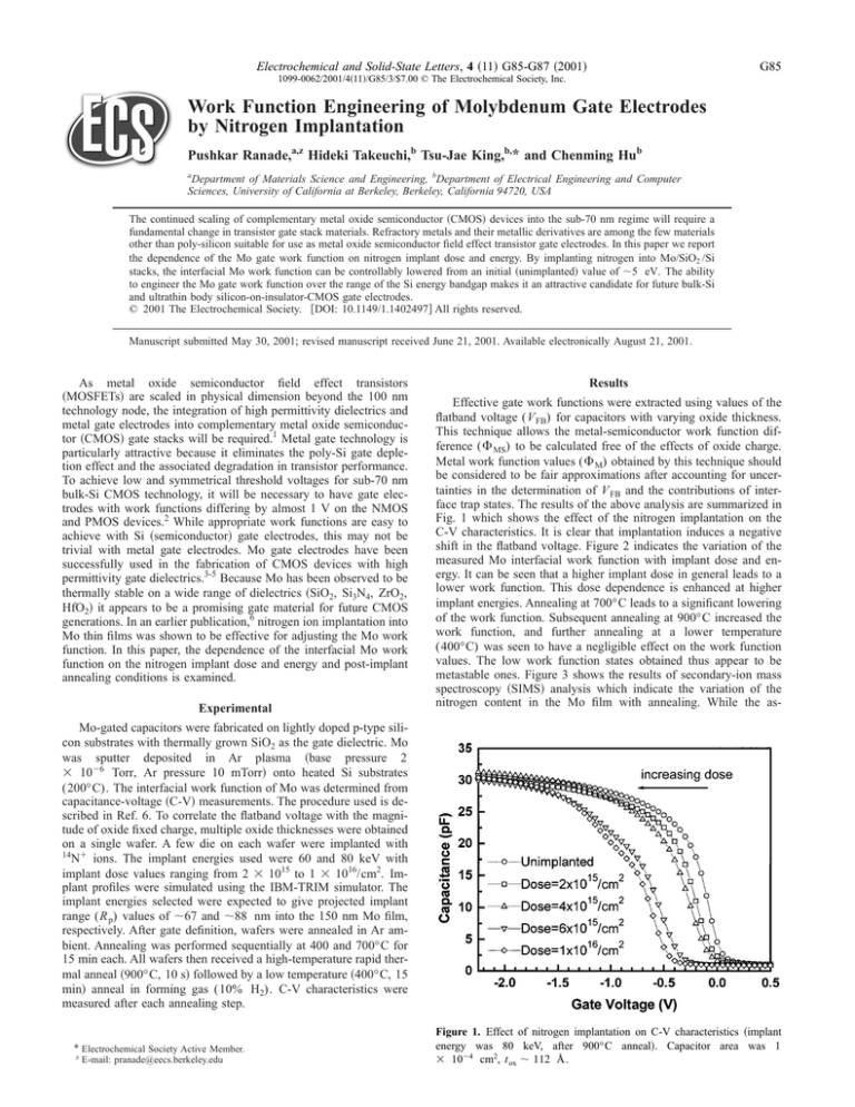
Fig. 1 which shows the effect of the nitrogen implantation on the
C-V characteristics. It is clear that implantation induces a negative
shift in the flatband voltage. Figure 2 indicates the variation of the
measured Mo interfacial work function with implant dose and energy. It can be seen that a higher implant dose in general leads to a
lower work function. This dose dependence is enhanced at higher
implant energies. Annealing at 700°C leads to a significant lowering
of the work function. Subsequent annealing at 900°C increased the
work function, and further annealing at a lower temperature
(400°C) was seen to have a negligible effect on the work function
values. The low work function states obtained thus appear to be
metastable ones. Figure 3 shows the results of secondary-ion mass
spectroscopy 共SIMS兲 analysis which indicate the variation of the
nitrogen content in the Mo film with annealing. While the as-
Mo-gated capacitors were fabricated on lightly doped p-type silicon substrates with thermally grown SiO2 as the gate dielectric. Mo
was sputter deposited in Ar plasma 共base pressure 2
⫻ 10⫺6 Torr, Ar pressure 10 mTorr兲 onto heated Si substrates
(200°C). The interfacial work function of Mo was determined from
capacitance-voltage 共C-V兲 measurements. The procedure used is described in Ref. 6. To correlate the flatband voltage with the magnitude of oxide fixed charge, multiple oxide thicknesses were obtained
on a single wafer. A few die on each wafer were implanted with
14 ⫹
N ions. The implant energies used were 60 and 80 keV with
implant dose values ranging from 2 ⫻ 1015 to 1 ⫻ 1016/cm2. Implant profiles were simulated using the IBM-TRIM simulator. The
implant energies selected were expected to give projected implant
range (R p) values of ⬃67 and ⬃88 nm into the 150 nm Mo film,
respectively. After gate definition, wafers were annealed in Ar ambient. Annealing was performed sequentially at 400 and 700°C for
15 min each. All wafers then received a high-temperature rapid thermal anneal 共900°C, 10 s兲 followed by a low temperature 共400°C, 15
min兲 anneal in forming gas (10% H2). C-V characteristics were
measured after each annealing step.
* Electrochemical Society Active Member.
z
E-mail: pranade@eecs.berkeley.edu
Figure 1. Effect of nitrogen implantation on C-V characteristics 共implant
energy was 80 keV, after 900°C anneal兲. Capacitor area was 1
⫻ 10⫺4 cm2, t ox ⬃ 112 Å.
G86
Electrochemical and Solid-State Letters, 4 共11兲 G85-G87 共2001兲
Figure 3. SIMS concentration-depth profiles for nitrogen, showing segregation at the Mo/SiO2 interface with annealing 共60 keV 14N⫹ implant, dose was
5 ⫻ 1015/cm2兲.
Figure 2. Variation of measured Mo work function with nitrogen implant
and annealing conditions. Also shown along the vertical axis are the positions of the conduction and valence bandedges of Si.
functions (⬃5 eV) observed from the unimplanted samples. The
work function lowering observed after 700°C annealing and the
subsequent increase in the work function after 900°C annealing can
be attributed to competing chemical changes 共nitrogen segregation兲
and structural changes 共improvement of crystalline quality兲 in the
film between these temperatures. The segregation of nitrogen at the
interface leads to an initial lowering of the work function 共annealing
at temperatures up to 700°C兲. While increasing the annealing temperature does increase the nitrogen concentration at the interface, it
also leads to an improvement in the crystalline quality of the film
and presumably increases the contribution of the 共110兲 Mo planes to
the work function. Thus, the subsequent increase in the work func-
implanted profile shows no distinct features, a significant pileup of
nitrogen is observed at the Mo/SiO2 interface after annealing at
700°C. This segregation effect is even more prominent after annealing at 900°C. Figure 4 shows the results of X-ray diffraction 共XRD兲
analysis performed on the Mo/SiO2 /Si stack after implantation. The
broad diffraction peak observed after implantation is indicative of
increased poly-crystallinity or nonuniform strain induced in the film.
Annealing at 700°C led to a fairly sharp and intense diffraction peak
and annealing at 900°C led to a further increase in the intensity of
the peak, indicating an improvement in the crystalline quality of the
film and the restoration of the predominantly 共110兲 texture of the
film.
Discussion
As seen in the cross-sectional SEM image of Fig. 5, the deposited Mo film has a columnar or fibrous morphology. XRD confirms
the predominantly 共110兲 texture 关共110兲 planes parallel to the surface兴
of this film. The various crystallographic planes of body-centered
cubic 共bcc兲 Mo crystals have vacuum work functions ranging from
4.3 to 4.95 eV.7 The 共110兲 Mo surfaces are the most densely packed
in the bcc system and possess the highest work functions. The columnar microstructure is thus crucial in obtaining the high work
Figure 4. XRD diffraction data showing evolution of Mo film morphology
after nitrogen implantation and annealing. The presence of a single diffraction peak at ⬃40.6° indicates a preferred 共110兲 texture to the Mo film.
Electrochemical and Solid-State Letters, 4 共11兲 G85-G87 共2001兲
G87
relatively straightforward technique to modulate the Mo work function over the range of the Si energy bandgap, so that Mo is an
attractive candidate gate electrode material for bulk-Si CMOS devices and also for ultrathin body SOI-CMOS devices.11
Conclusions
The effect of nitrogen implantation and thermal annealing on the
work function of Mo gate electrodes is presented. Nitrogen is observed to segregate at the Mo/SiO2 interface upon thermal annealing, lowering the interfacial Mo work function from a relatively
high value of ⬃5 eV. The ability to tailor the Mo work function
over a fairly wide range makes it an attractive candidate for future
CMOS technology generations.
References
Figure 5. Cross-sectional SEM image showing morphology of deposited
Mo film.
tion is observed to be dependent on the implant dose and energy and
the resulting crystalline damage induced by the implant. An optimization of the implant dose and energy will hence be necessary to
control the final work function.
Metal work functions at dielectric interfaces have been observed
to be dependent on the permittivity of the dielectric.8-10 While the
interfacial Mo work function does vary with the dielectric being
used,3-6 the variation is within 200 mV of the vacuum surface work
function of the 共110兲 crystallographic planes of Mo 共4.95eV兲.7 This
observation indicates the applicability of Mo as a bulk-Si PMOS
gate electrode. Selective nitrogen implantation into the Mo film is a
1. International Technology Roadmap for Semiconductors, Semiconductor Industry
Association, 1999.
2. I. De, D. Johri, A. Srivastava, and C. M. Osburn, Solid-State Electron., 44, 1077
共2000兲.
3. Q. Lu, R. Lin, P. Ranade, Y.-C. Yeo, X. Meng, H. Takeuchi, T.-J. King, C. Hu, H.-F.
Luan, S. Lee, W. Bai, C.-H. Lee, D.-L. Kwong, X. Guo, X. Wang, and T.-P. Ma,
Tech. Dig. Int. Electron Devices Meet., 2000, 641.
4. Y.-C. Yeo, Q. Lu, P. Ranade, H. Takeuchi, K. J. Yang, I. Polishchuk, T.-J. King, C.
Hu, S. C. Song, H. F. Luan, and D.-L. Kwong, IEEE Electron Device Lett., 22, 227
共2001兲.
5. Q. Lu, R. Lin, P. Ranade, T.-J. King, and C. Hu, in VLSI Technology Digest, p. 45,
IEEE, New York 共2001兲.
6. P. Ranade, Y.-C. Yeo, Q. Lu, H. Takeuchi, T.-J. King, C. Hu, in Gate Stack and
Silicide Issues in Silicon Processing, C3.2.1, MRS, Warrendale, PA 共2000兲.
7. H. B. Michaelson, J. Appl. Phys., 48, 4729 共1977兲.
8. Y.-C. Yeo, P. Ranade, Q. Lu, R. Lin, T.-J. King, and C. Hu, in VLSI Technology
Digest, p. 49, IEEE, New York 共2001兲.
9. R. C. Keller and C. R. Helms, J. Vac. Sci. Technol. A, 10, 775 共1992兲.
10. H. Matsuhashi and S. Nishikawa, Jpn. J. Appl. Phys., Part 1, 33, 1293 共1994兲.
11. L. Chang, S. Tang, T.-J. King, J. Bokor, and C. Hu, Tech. Dig. Int. Electron Devices
Meet., 719 共2000兲.


