1 The paper investigates the implementation of the current-
advertisement
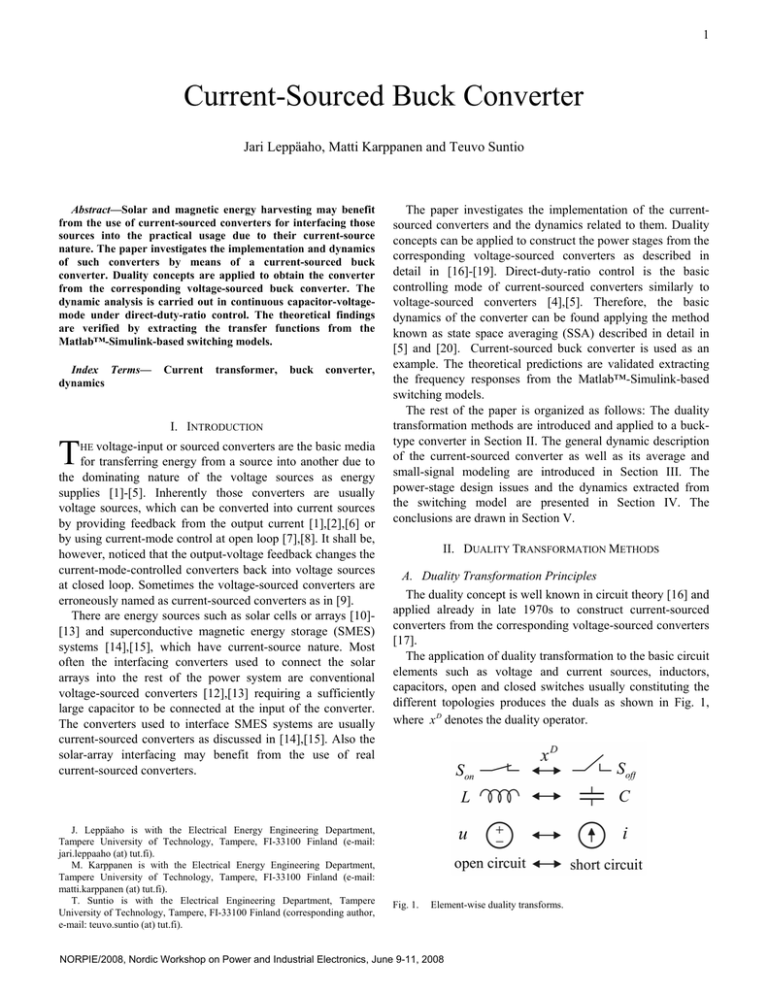
1 Current-Sourced Buck Converter Jari Leppäaho, Matti Karppanen and Teuvo Suntio Abstract—Solar and magnetic energy harvesting may benefit from the use of current-sourced converters for interfacing those sources into the practical usage due to their current-source nature. The paper investigates the implementation and dynamics of such converters by means of a current-sourced buck converter. Duality concepts are applied to obtain the converter from the corresponding voltage-sourced buck converter. The dynamic analysis is carried out in continuous capacitor-voltagemode under direct-duty-ratio control. The theoretical findings are verified by extracting the transfer functions from the Matlab™-Simulink-based switching models. Index Terms— dynamics T Current transformer, buck converter, I. INTRODUCTION HE voltage-input or sourced converters are the basic media for transferring energy from a source into another due to the dominating nature of the voltage sources as energy supplies [1]-[5]. Inherently those converters are usually voltage sources, which can be converted into current sources by providing feedback from the output current [1],[2],[6] or by using current-mode control at open loop [7],[8]. It shall be, however, noticed that the output-voltage feedback changes the current-mode-controlled converters back into voltage sources at closed loop. Sometimes the voltage-sourced converters are erroneously named as current-sourced converters as in [9]. There are energy sources such as solar cells or arrays [10][13] and superconductive magnetic energy storage (SMES) systems [14],[15], which have current-source nature. Most often the interfacing converters used to connect the solar arrays into the rest of the power system are conventional voltage-sourced converters [12],[13] requiring a sufficiently large capacitor to be connected at the input of the converter. The converters used to interface SMES systems are usually current-sourced converters as discussed in [14],[15]. Also the solar-array interfacing may benefit from the use of real current-sourced converters. J. Leppäaho is with the Electrical Energy Engineering Department, Tampere University of Technology, Tampere, FI-33100 Finland (e-mail: jari.leppaaho (at) tut.fi). M. Karppanen is with the Electrical Energy Engineering Department, Tampere University of Technology, Tampere, FI-33100 Finland (e-mail: matti.karppanen (at) tut.fi). T. Suntio is with the Electrical Engineering Department, Tampere University of Technology, Tampere, FI-33100 Finland (corresponding author, e-mail: teuvo.suntio (at) tut.fi). The paper investigates the implementation of the currentsourced converters and the dynamics related to them. Duality concepts can be applied to construct the power stages from the corresponding voltage-sourced converters as described in detail in [16]-[19]. Direct-duty-ratio control is the basic controlling mode of current-sourced converters similarly to voltage-sourced converters [4],[5]. Therefore, the basic dynamics of the converter can be found applying the method known as state space averaging (SSA) described in detail in [5] and [20]. Current-sourced buck converter is used as an example. The theoretical predictions are validated extracting the frequency responses from the Matlab™-Simulink-based switching models. The rest of the paper is organized as follows: The duality transformation methods are introduced and applied to a bucktype converter in Section II. The general dynamic description of the current-sourced converter as well as its average and small-signal modeling are introduced in Section III. The power-stage design issues and the dynamics extracted from the switching model are presented in Section IV. The conclusions are drawn in Section V. II. DUALITY TRANSFORMATION METHODS A. Duality Transformation Principles The duality concept is well known in circuit theory [16] and applied already in late 1970s to construct current-sourced converters from the corresponding voltage-sourced converters [17]. The application of duality transformation to the basic circuit elements such as voltage and current sources, inductors, capacitors, open and closed switches usually constituting the different topologies produces the duals as shown in Fig. 1, where x D denotes the duality operator. Fig. 1. Element-wise duality transforms. NORPIE/2008, Nordic Workshop on Power and Industrial Electronics, June 9-11, 2008 2 Different electric circuits can be presented by using graphs, where each arc represents a certain circuit element in the selected topology. In this case, the voltage-input circuit is naturally the base from which the first graph will be constructed. The dual of the graph can be constructed in such a way that the arcs connected in series in the original graph will be connected in parallel in the dual of the graph and the parallel connected arcs in series, respectively. The corresponding current-input circuit will be obtained from the graph by connecting the duals of the elements (Fig. 1) as the graph dictates. These procedures are illustrated in Fig. 2 based on a simple LC -filter circuit. Applying the methods described above in Subsection A, the graph of the voltage-input buck converter in Fig. 3b can be transformed into its dual as shown in Fig. 4a. The arcs of the dual of the graph determine the elements and their connections and thus the topology of the current-input buck converter as shown in Fig. 4b. Fig. 4. Current-input buck converter: a) Graph and b) Schematics. III. DYNAMIC REPRESENTATIONS Fig. 2. LC -filter: a) Voltage-input schematics, b) Its graph, c) The dual of the graph and d) Current-input schematics. The dynamics of the voltage-input-voltage-output converter can be represented by means of a linear two-port network with G-parameters (Fig. 5) [2],[3],[20], which constitute the set of transfer functions given by B. Current-Input Buck Converter A conventional voltage-input buck converter with synchronous rectification is shown in Fig. 3a. The corresponding graph, where Son denotes the high-side MOSFET and Soff the low-side MOSFET, is shown in Fig. 3b. Fig. 3. ⎡ iˆin ⎤ ⎡ Yin ⎢ ⎥=⎢ ⎣uˆo ⎦ ⎣Gio where [îin uˆo ] denotes T Toi −Zo the ⎡uˆ ⎤ Gci ⎤ ⎢ in ⎥ iˆ Gco ⎥⎦ ⎢ o ⎥ ⎢⎣ cˆ ⎥⎦ output T (1) vector and ⎡uˆin iˆo cˆ ⎤ the input vector (See Fig. 3a). The general ⎣ ⎦ control variable is denoted by ĉ . The transfer functions in (1) represent the pure internal dynamics, where the load and source effects are eliminated. Voltage-input buck converter: a) Schematics and b) Graph. Fig. 5. Linear two-port network with G-parameters. 3 The dynamics of the current-input-current-output converter can be represented by means of a linear two-port network with H-parameters [20] (Fig. 6), which constitutes the set of transfer functions given by ⎡uˆin ⎤ ⎡ Z in ⎢ iˆ ⎥ = ⎢G ⎣ o ⎦ ⎣ io where ⎡uˆin ⎣ T iˆo ⎤⎦ denotes Toi −Yo the ⎡ iˆ ⎤ Gci ⎤ ⎢ in ⎥ uˆ Gco ⎥⎦ ⎢ o ⎥ ⎢ cˆ ⎥ ⎣ ⎦ output (2) vector and T ⎡iˆin uˆo cˆ ⎤ denotes the input vector (See Fig. 4b). The ⎣ ⎦ general control variable is denoted by ĉ . Similarly to the voltage-input converter, the transfer functions in (2) represent the internal dynamics of the current-input converter. Fig. 6. low-side MOSFET conducts and the corresponding topological circuit structure is shown in Fig. 8b, respectively. Fig. 7. Current-input synchronous buck converter. Fig. 8. Current-input buck converter during the a) on time and b) off time. Linear two-port network with H-parameters. A. Average and Small-Signal Modeling The average and small-signal modeling of a current-input converter can be done similarly to the voltage-input converter by applying state-space-averaging (SSA) technique introduced in detail in [5] and [21]. We consider the converter to operate in continuous conduction mode (CCM), which means that the capacitor voltages are continuous similarly to the inductor currents in the voltage-input converters. The state variables of the system are the time-averaged values of the capacitor voltages and inductor currents [21]. In order to construct the averaged state space, we have to solve the derivatives of the capacitor voltages and inductor currents during the on and off times. The averaging is carried out by multiply the on-time equations with the duty ratio d and the off-time equations with the complement of the duty ratio d ′ and summing them together. Similar procedures are applied to the output variables ( uin and io ) for obtaining the output equations. The small-signal state space can be obtained from the averaged state space by developing the proper partial derivatives, i.e., by linearizing the averaged state space [21]. The open-loop current-input buck converter with the relevant parasitic elements is shown in Fig. 7. During the on time, the high-side MOSFET conducts and the corresponding topological circuit is shown in Fig. 8a. During the off time, the Applying the above described procedures and Kirchhoff’s voltage and current laws, the averaged state space can be given by d ⟨uC ⟩ 1 d = − ⟨iL ⟩ + ⟨iin ⟩ dt C C r +r dr d ⟨iL ⟩ 1 1 = ⟨uC ⟩ − L C ⟨iL ⟩ + C ⟨iin ⟩ − ⟨uo ⟩ dt L L L L ⟨uin ⟩ = d ⟨uC ⟩ − drC ⟨iL ⟩ + (drds1 + d ′rds 2 + drC )⟨iin ⟩ (3) ⟨io ⟩ = ⟨iL ⟩ The steady-state operating point can be solved from (3) by letting the derivatives to be zero. These procedures yield I o = DI in U C = U o + DrL I in (4) U in = DU o + ( D rL + DD ′rC + Drds1 + D′rds 2 ) I in 2 The small-signal state space can be solved from (3) by developing the proper partial derivatives, which yields 4 duˆC I D 1 = − iˆL + iˆin + in dˆ dt C C C ˆ r +r Dr r I diL 1 1 = uˆC − L C iˆL + C iˆin − uˆo + C in dˆ dt L L L L L uˆin = DuˆC − DrC iˆL + r1iˆin + U1dˆ the corresponding voltage-input converter constituting the Gparameter set in (1) as follows (21): (5) iˆo = iˆL where U1 = U o + ( DrL + D′rC + rds1 − rds 2 ) I in r1 = DrC + Drds1 + D ′rds 2 A small-signal two-port model similar to the canonical equivalent circuit provided in [5] can be constructed from the small-signal state space in (5) as shown in Fig. 9. The parameters eˆ( s ) , ˆj ( s ) and re can be given by eˆ( s ) = U o + ( DrL + (1 − 2 D)rC + rds1 − rds 2 ) I in ˆj ( s ) = I in D (6) re = Drds1 + D′rds 2 + DD ′rC ⎡ Yin − o ⎢G ⎣ io − o 2 ⎤ D(1 + srC C ) 1 ⎡ D sC ⎢ ⎥ LC ⎣ D(1 + srC C ) −(rL + Drds1 + D′rds 2 + sL)(1 + srC C ) ⎦ (8) r + Drds1 + D ′rds 2 + rC 1 s2 + s L + L LC D U r r I sC ( ( ) ) + − ⎤ 1 ⎡ in ds 2 ds1 o ⎢ ⎥ ⎡ Gci ⎤ LC ⎣(U in + (rds 2 − rds1 ) I o )(1 + srC C ) ⎦ ⎡ I o ⎤ = +⎢ ⎥ ⎢G ⎥ ⎣0⎦ ⎣ co ⎦ s 2 + s rL + Drds1 + D ′rds 2 + rC + 1 L LC The small-signal equivalent circuit [5] for the voltage-input buck converter can be given as shown in Fig. 10, where the parameters eˆ( s ) , ˆj ( s ) and re can be given by U in − (rds1 − rds 2 ) I o D re = rL + Drds1 + D′rds 2 eˆ( s ) = Fig. 9. Toi − o ⎤ = − Z o − o ⎥⎦ ˆj ( s ) = I o (9) Small-signal equivalent circuit of the current-input buck converter. The transfer functions constituting the H-parameters in (2) can be solved from (5) in Laplace domain by utilizing the conventional matrix manipulation methods. These procedures yield the open-loop transfer functions as follows: ⎡ Z in − o ⎢G ⎣ io − o Toi − o ⎤ = −Yo − o ⎥⎦ 2 2 1 ⎡ D ( s ( L − rC C ) + rL − rC ) D(1 + srC C ) ⎤ ⎢ ⎥ LC ⎣ − sC D(1 + srC C ) ⎦ + ⎡ r1 0 ⎤ (7) ⎢ 0 0⎥ r +r 1 ⎣ ⎦ s2 + s L C + L LC 2 1 ⎡ DI in ( s ( L − rC C ) + rL − rC ) ⎤ ⎢ ⎥ I in (1 + srC C ) ⎡ Gci ⎤ LC ⎣ ⎦ + ⎡U1 ⎤ = ⎢G ⎥ ⎢0⎥ r r + 1 2 ⎣ ⎦ ⎣ co ⎦ s +s L C + L LC For comparison, we give the open-loop transfer functions of Fig. 10. Small-signal equivalent circuit of the voltage-input buck converter. The small-signal equivalent circuits shown in Figs. 9 and 10 offer excellent physical insight into the internal dynamics of the converters and thereby, reveal explicitly the similarities and differences they have in terms of internal dynamics. IV. PRACTICAL DESIGN AND DYNAMIC ISSUES The inductors in a voltage-input converter are typically chosen allowing a certain peak-to-peak ripple current to appear in an inductor, which is in the order of 20-40 % of their average current. The output capacitor is chosen such that the output-voltage dip will be less than a certain value, when the output current is changed step-wisely for a certain amount. Similar methods can be also applied in the case of the currentinput converter but the ripple definition will be applied to the capacitors and the transient specifications to obtain the value of the output inductor, respectively. 5 The ripple voltage of the capacitor is triangular shaped, because it is charged and discharged by means of effectively constant currents. The up slope of the voltage ( m1 ) can be iin − iL i and the down slope ( m2 ) by L . This means C C that the peak-to-peak ripple voltage can be given by given by DTs ( I in − I o ) C and the average slope of the capacitor voltage by ΔuC − pp = d ⟨uC ⟩ D⟨iin ⟩ − ⟨io ⟩ = dt C (10) (11) The value of the capacitor ( C ) can be naturally solved according to (10), when the ripple value is specified. The output-voltage step change ( ΔU o ) causes DC voltage Fig. 11. a) Main simulation set-up and b) PWM-block model. to appear over the inductor for a time Δt = ΔU o /(d ⟨uC ⟩ / dt ) . The resulting volt-seconds Δλ = Δt ⋅ ΔU o / 2 would cause an undershoot or overshoot in the output current, which can be given by Δio = Δλ / L (12) The value of the output inductor ( L ) can be naturally solved according to (12), when the transient specifications are given. A. Circuit Element Selection The design of the converter will be carried out by using the following specifications: I in = 1 - 2 A , Uo = 3 - 5 V , I o = 0.5 A and f s = 100 kHz . The allowed capacitor-voltage peak-to-peak ripple is 20 % of the nominal value and the output-current dip 10 % of the nominal value, respectively. These specifications yield C ≈ 10 μF (Eq. (10)) and L ≈ 500 μH (Eq. (12)). The circuit parasitic elements are taken as follows: rL = 0.2 Ω , rC = 30 mΩ and rds1 = rds 2 = 0.2 Ω . The simulations have been carried out by using Matlab™ Simulink Toolbox, where the switching models are constructed by means of the on and off-time state spaces (Fig. 8), which are implicitly observable also in (5): Fig. 11a shows the main simulation set-up and Fig. 11b the PWM-modulator block. Fig. 12 shows the power-stage models. The simulated capacitor voltage and output current are shown in Figs. 13 and 14. The capacitor-voltage waveforms resemble the inductor-current waveforms typically observed in a voltage-input converter and the output-current waveforms the output-capacitor waveforms, respectively. These phenomena are expected due to the applied duality transformations, when constructing the current-input converter. Fig. 12. Power-stage simulation models: a) Main set-up, b) Inductor-current block and c) Capacitor-voltage block. 6 B. Dynamic Evaluation The dynamic evaluation of the predicted transfer functions in (7) is basically done in such a way that a sinus signal is injected on the top of the original input signal into the port serving as the excitation input and the corresponding respond is recorded from the port serving as the response output. The single-frequency value of the impulse response is computed based on the response and injection data applying Fast Fourier Transformation (FFT) method. A Matlab™ script is constructed to execute the required FFT procedures. The frequency range of interest is scanned with an appropriate number of injections. The control-to-output transfer function ( Gco ), input-to-output transfer function ( Gio − o ) and the output Control-to-Output The frequency responses of the control-to-output transfer function ( Gco ) are shown in Fig. 15 at the input current of 1 A and 2 A, respectively. The responses resemble the corresponding responses of the voltage-input converter. The dots denote the switching-model-based (Figs. 11 and 12) responses, which coincide exactly with the predicted responses (7). admittance ( Yo − o ) are subjected for the evaluation. Similarly to the VMC-controlled voltage-input converter operating in CCM, the VMC-controlled current-input converter would exhibit resonant behavior having resonant frequency at 2.25 kHz. Fig. 15. Control-to-output transfer functions at the input current of 1 A (dashed line) and 2 A (solid line). Input-to-Output Fig. 13. Capacitor-voltage waveforms at the input current of 1 A and 2 A. Fig. 14. Output-current waveforms at the input current of 1 A and 2 A. The frequency responses of the input-to-output transfer function ( Gio − o ) are shown in Fig. 16 at the input current of 1 A and 2 A. The responses resemble the responses of the corresponding voltage-input converter. The dots denote the switching-model-based responses coinciding exactly with the predicted responses (7). Fig. 16. Input-to-output transfer function at the input current of 1 A (dashed line) and 2 A (solid line). 7 Output Admittance [7] The frequency response of the output admittance is shown in Fig. 17, where the dots denote the switching-model-based responses. The shape of the response corresponds to the input admittance of the voltage-input converter not the output impedance. [8] [9] [10] [11] [12] [13] [14] [15] [16] [17] [18] Fig. 17. Output admittance. [19] V. CONCLUSIONS The paper investigated the implementation and dynamic modeling of current-input converters. Buck-type converter was used as an example. It was shown that the duality principles and graph technique can be used to obtain the power stage of the current-input converter from the corresponding voltage-input converter. The dynamic models of the direct-duty-ratio control can be obtained by applying stage-space averaging yielding accurate models up to the half the switching frequency. The obtained frequency responses resemble the responses of the voltage-input converter. The practical problems with the current-input converters would be related to the auxiliary-power generation. REFERENCES [1] [2] [3] [4] [5] [6] Y. Huang and C. K. Tse, “Circuit theoretic classification of parallel connected converters DC-DC converters,” IEEE Trans. on Circuits and Systems -I: Regular Papers, vol. 54, no. 5, May 2007, pp. 1099-1108. T. Roinila, M. Hankaniemi, T. Suntio, M. Sippola and M. Vilkko, “Dynamical profile of a switched-mode converter – Reality or imagination,” in Proc. IEEE INTELEC’07, 2007, pp. 420-427. T. Suntio, M. Hankaniemi and M. Karppanen, “Analysing the dynamics of regulated converters,” IEE Proc. Electric Power Applications, vol. 153, no. 6, November 2006, pp. 905-910. G. W. Wester and R. D. Middlebrook, “Low-frequency characterization of switched-dc-dc converters,” IEEE Trans. on Aerospace and Electronic Systems, vol. AES-9, no. 3, May 1973, pp. 376-385. R. D. Middlebrook and S. ´Cuk, “A general unified approach to modeling switching-converter power stages,’ Int. Journal of Electronics, vol. 42, no. 6, 1977, pp. 521-550. M. Hankaniemi and T. Suntio, “Dynamical modeling and control of current-output converters,” International Review of Electrical Engineering, vol. 4, no. 5, September-October 2007, pp. 671-680. [20] [21] C. W. Deisch, “Simple switching control method changes power converter into a current source,” in Proc. IEEE PESC’78, 1978, pp. 300306. T. Suntio and M. Karppanen, “Methods to characterize open-loop dynamics of current-mode-controlled converters,” in Proc. IEEE PESC’08, 2008 (in press). W. W. Weaver and P. T. Krein, “Analysis and application of a currentsourced buck converter,“ in Proc. IEEE APEC’07, 2007, pp. 1664-1670. S. Liu and R. A. Dougal, “Dynamic multiphysics model for solar array,” IEEE Trans. on Energy Conversion, vol. 17, no. 2, June 2002, pp. 285294. D. Sera, R. Teoderescu and P. Rodriguez, “PV panel model based on data sheet values,” in Proc. IEEE ISIE’07, 2007, pp. 2392-2396. W. Xiao, W. G. Dunford, P. R. Palmer and A. Capel, “Regulation of photovoltaic voltage,” IEEE Trans. on Industrial Electronics, vol. 54, no. 3, June 2007, pp. 1265-1374. W. Xiao, N. Ozog and W. G. Dunford, “Topology study of photovoltaic interface for maximum power point tracking,” IEEE Trans. on Industrial Electronics, vol. 54, no. 3, June 2007, pp. 1696-1704. R. W. Boom and H. A. Peterson, “Superconductive energy storage for power systems,” IEEE Trans. on Magnetics, vol. MAG-8, no. 3, September 1972, pp. 701-703. D. Shmilovitz and S. Singer, “A switched mode converter suitable for superconductive magnetic energy storage (SMES) systems,’ in Proc. IEEE APEC’02, 2002, pp. 630-634. C. A. Desoer and E. S. Kuh, “Basic Circuit Theory,” McGraw-Hill: New York, NY, USA, 1969. S. ´Cuk, “General topological properties of switching structures,” in Proc. IEEE PESC’79, 1979, pp. 109-130. D. Shmilovitz, “Application of duality for derivation of current converter topologies,” HIT Journal of Science and Engineering B, vol. 2, nos. 3-4, pp. 529-557. R. Rabinovici and B. Z. Kaplan, “Novel DC-DC converter schemes obtained through duality principle and topological considerations,” IEE Electronics Letters, vol. 27, no. 21, October 1991, pp. 1948-1950. C. K. Tse, ‘Linear Circuit Analysis,’ Addison Wesley Longman, Harlow, England, 1998. T. Suntio, “Unified average and small-signal modeling of direct-on-time control,” IEEE Trans. on Industrial Electronics, vol. 53, no. 1, February 2006, pp. 287-295.
