Chapter 4: Electronic Signal Processing
advertisement

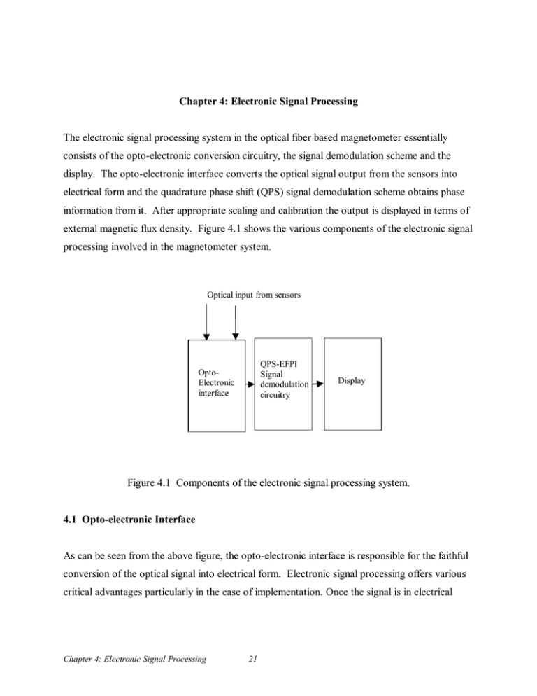
Chapter 4: Electronic Signal Processing The electronic signal processing system in the optical fiber based magnetometer essentially consists of the opto-electronic conversion circuitry, the signal demodulation scheme and the display. The opto-electronic interface converts the optical signal output from the sensors into electrical form and the quadrature phase shift (QPS) signal demodulation scheme obtains phase information from it. After appropriate scaling and calibration the output is displayed in terms of external magnetic flux density. Figure 4.1 shows the various components of the electronic signal processing involved in the magnetometer system. Optical input from sensors QPS-EFPI Signal demodulation circuitry OptoElectronic interface Display Figure 4.1 Components of the electronic signal processing system. 4.1 Opto-electronic Interface As can be seen from the above figure, the opto-electronic interface is responsible for the faithful conversion of the optical signal into electrical form. Electronic signal processing offers various critical advantages particularly in the ease of implementation. Once the signal is in electrical Chapter 4: Electronic Signal Processing 21 domain, techniques like amplification and filtering can be easily applied in order to enhance the signal to noise ratio (SNR) of the system. Not only is this important, particularly in high resolution systems, but necessary in the magnetometer system. Thus, the most important requirement on the interface circuitry is the accurate reproduction of the optical signal in electrical form with the addition of minimal external noise. Figure 4.2 shows the circuit diagram of the pre-amplifier circuitry. Cf Rf - Pin I Vout + + Figure 4.2 Schematic of a single-channel preamplifier circuit. The optical signal returning from the sensor is incident on the PIN diode thus inducing a reverse photo current in it. This current flows through the feedback resistor causing a voltage drop across it. The current flowing through the diode is directly proportional to the intensity of the optical input. Low input current and offset voltage levels are the most important requirements on the operational amplifiers used in such sensitive photodiode applications. The first stage of the preamplifier circuit is thus a current to voltage converter or a trans-impedance amplifier. The second stage of the preamplifier circuit is a voltage follower with high input and low output impedance. This stage prevents subsequent stages from loading the preamplifier circuitry. In a typical preamplifier circuit shown in Figure 4.2 above, the output of the amplifier is given by Equation 4.1. Chapter 4: Electronic Signal Processing 22 Vout = Pin.R.Rf (4.1) where Pin is the incident optical power in watts, Rf is the value of the feedback resistor in ohms and R is the responsivity or sensitivity of the PIN photodiode (unit Amp/Watt). An equivalent model for a photodiode and its dc error sources is shown in Figure 4.3. Cf Rf Photodiode RD ID Vos CD IB + Output Figure 4.3 Equivalent photodiode model with dc error sources. The amplifier’s input current, IB, contributes to an output voltage error which is proportional to the value of the feedback resistor. The offset voltage error, VOS, causes a dark current error due to the photodiode’s finite shunt resistance, RD. The resulting output voltage error, VE, is given by Equation 4.2 as, VE=(1+Rf/RD)VOS+RfIB (4.2) In order to prevent the generation of unwanted noise signals in the preamplifier, the optoelectronic conversion circuitry is encased in an EMI resistant enclosure. In addition to shielding the circuit from EMI, the aluminum enclosure offers mechanical protection to internal components like photodiodes. Chapter 4: Electronic Signal Processing 23 4.2 Quadrature Phase Shifted EFPI Signal Demodulation Scheme Once the sensor output is converted into electrical form, Quadrature Phase Shift (QPS) signal demodulation scheme is employed in order to detect the phase signal. This technique ensures the signal phase detection regardless of the initial phase of the sensor. The technique uses two sensors which are 90o out of phase or “in quadrature”. For these two sensors, the output voltage can be approximated by Eqs. 4.3 and 4.4. and Vout1 = Vdc1 + Vmax 1(1 + cos(ϕ )) , (4.3) Vout 2 = Vdc 2 + Vmax 2 (1+ sin(ϕ )) , (4.4) where ϕ is the phase difference between the two reflected beams. When the change in the phase, ∆ϕ , is small, the following approximations hold. and ∆ Vout1 = − Vmax 1 sin ϕ ∆ ϕ , (4.5) ∆ Vout 2 = Vmax 2 cos ϕ ∆ ϕ . (4.6) Defining a signal S in the following way, S = (Vout 1 ) + (Vout 2 ) , (4.7) S ∝ ∆ϕ . (4.8) 2 2 and adjusting Vmax1 equal to Vmax2, Thus the output signal S , is linearly proportional to the change in phase signal and independent of its initial value, for small phase changes. Each sensor can be brought to its initial operating Chapter 4: Electronic Signal Processing 24 point by adjusting the initial air gap. A block diagram of the signal demodulation system (for a single axis) is as shown in Figure 4.4. Laser source and opto-electronic interface Signal demodulation and display system Amplifier Differentiator Square & add Display Scale Square root Figure 4.4 Block diagram of QPS signal demodulation scheme. 4.3 Analog Implementation The signal demodulation scheme explained above can be electronically implemented in either analog or digital domain. This section details the analog implementation of the scheme. Figs. 4.5 (a) and 4.5 (b) show the block and circuit schematic of this system. Chapter 4: Electronic Signal Processing 25 Buffer + Divider IP1 Amplifier ( )2 V01 Input from laser source + Display V02 - IP2 Buffer + Divider Amplifier ( )2 Figure 4.5 (a) Analog implementation of QPS signal demodulation scheme. As shown in the figure, the electrical sensor outputs from the interface circuit are first normalized to the laser diode output using linear divider integrated circuits (ICs). This eliminates the low frequency noise in the system arising due to variation in the laser output power. These normalized signals are then differentiated by subtracting their initial signal values from the current ones. The subtraction is carried out using operational amplifiers. These differentiated sensor outputs are then squared using linear multiplier ICs and added. The square root of this summed signal is then scaled, calibrated and displayed in terms of external magnetic flux density. Although an analog system implementation is simple in design and fabrication, it has several major disadvantages, some of which are given below. Chapter 4: Electronic Signal Processing 26 +15 V R R 10K Rf -15 V + ÷ Sensor 1 o/p R1 + R + R R 2R Input From Laser Source ( )2 + √ Display Subtractor R R R +15 V R R 10K Rf -15 V + ÷ Sensor 2 o/p Buffer + R R1 + ( )2 R Divider Differentiator Amplifier Square Figure 4.5 (b) Circuit schematic of the demodulation system. • Additional thermal noise generated in the circuit degrades the SNR of the overall system. • Components like resistors and capacitors, with precise values, are generally not easily available. Chapter 4: Electronic Signal Processing 27 • Linear integrated circuits like multipliers and dividers have inherent inaccuracy in the computed signal output. • Fabrication of the circuit, although simple, is time consuming. • The system implementation is not flexible as modification is difficult. Since SNR, accuracy, flexibility and speed are critical in the ultra-high sensitivity magnetometer system, it is clear from the above discussion, that analog implementation of the signal demodulation scheme is not suitable for this particular application. Thus a microprocessorbased, digital signal demodulation scheme is used in the final magnetic field measuring system. The next section describes the various advantages and implementation of this system. 4.4 Microprocessor-based Signal Demodulation A microprocessor based signal demodulation scheme is used in the final magnetometer system. This increases the signal processing accuracy and eliminates manual calibration of the individual sensors as well as increases system reliability and flexibility. Figure 4.6 below shows the schematic of the digital implementation. ADC Optoelectronic I/F CPU MUX Memory Display Figure 4.6 Schematic of microprocessor-based signal demodulation system. Chapter 4: Electronic Signal Processing 28 The electrical signals from the sensors and the normalizing input from the laser source are all fed into the 16X1 multiplexer through the opto-electronic interface. The analog to digital converter (ADC) converts each signal into a 12 bit word. The central processing unit (CPU) performs all the calculations like normalizing, differentiating, squaring and adding on this data and displays the results on a LCD panel. The software instructions for the signal processing are stored in the memory and can be directly accessed by the microprocessor. The stand-alone, single board computer (SBC) chosen for this application is based on Intel’s 386EX CPU with a clock speed of 25 MHz. The output from the three pairs of sensors (one pair for each Cartesian axis) and the normalizing input is fed to the computer through a 16 channel, 12-bit ADC with an input range of 0-10 V. The resolution of the ADC is thus around 2 mV. The overall sampling rate can be as high as 100 KHz. Once the input data is obtained in digital form, all the operations required for quadrature phase shift demodulation are performed on it. The output is displayed on a 4X20 character LCD panel. The SBC can be programmed for selfcalibration or can be calibrated either on start-up or during operation. The operation of the SBC can be altered whenever required by downloading new executable files from a PC through a serial port and RS232 cable. Thus the system offers much higher operational flexibility as compared to analog signal demodulation. Some of the significant advantages of the microprocessor-based system are as shown below. • Significant reduction in thermal noise as output of preamplifier is directly converted to digital format without further analog processing. • Increase in system reliability as commercially available single board computer is used for the signal demodulation scheme. • Sufficient resolution for the required application. Chapter 4: Electronic Signal Processing 29 • Flexible operation, since this simply involves modification of software. • Faster implementation as this only requires downloading of modified executable file on to the single board computer. Specifications of some of the critical components of the microprocessor-based signal demodulation system are as shown below. 1. Analog to Digital Converter • 16 single ended channels • 12 bit output, a resolution of 2.44 mV for 0-10V input signal • Absolute. accuracy of +/- 1 LSB or 2.44 mV • Sampling rate 6.25 KHz/channel which is more than adequate for DC signal measurement. 2. Single Board Computer • Stand-alone operation • Externally programmable • Intel 386EX CPU • 25 MHz clock speed • Can be hooked up to a personal computer through a serial port for code debugging and downloading. Chapter 4: Electronic Signal Processing 30


