Scanning Tunneling Microscopy and Spectroscopy of Gallium Oxide
advertisement

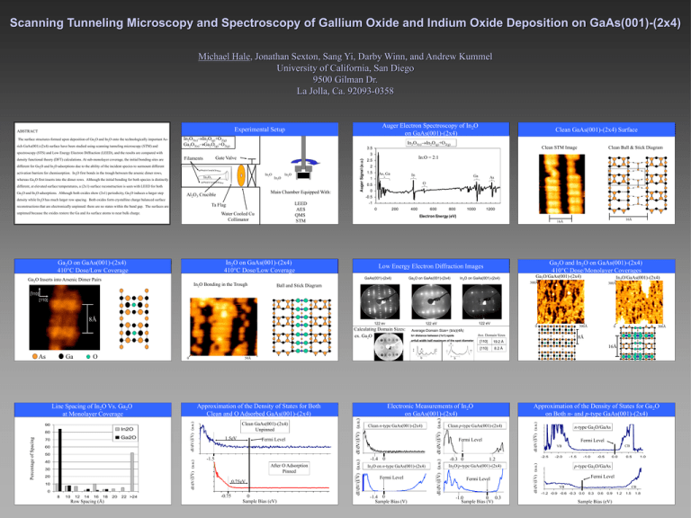
Scanning Tunneling Microscopy and Spectroscopy of Gallium Oxide and Indium Oxide Deposition on GaAs(001)-(2x4) Michael Hale, Jonathan Sexton, Sang Yi, Darby Winn, and Andrew Kummel University of California, San Diego 9500 Gilman Dr. La Jolla, Ca. 92093-0358 Auger Electron Spectroscopy of In2O on GaAs(001)-(2x4) Experimental Setup ABSTRACT The surface structures formed upon deposition of Ga2O and In2O onto the technologically important Asrich GaAs(001)-(2x4) surface have been studied using scanning tunneling microscopy (STM) and In2O3(s)In2O(g)+O2(g) Ga2O3(s)Ga2O(g)+O2(g) In2O3(s)In2O(g)+O2(g) different for Ga2O and In2O adsorptions due to the ability of the incident species to surmount different activation barriers for chemisorption. In2O first bonds in the trough between the arsenic dimer rows, In2O In2O3 whereas Ga2O first inserts into the dimer rows. Although the initial bonding for both species is distinctly In2O In2O different, at elevated surface temperatures, a (2x1) surface reconstruction is seen with LEED for both Ga2O and In2O adsorptions. Although both oxides show (2x1) periodicity, Ga2O induces a larger step Main Chamber Equipped With: Al2O3 Crucible In:O = 2:1 2.5 2 1.5 As, Ga In 1 Water Cooled Cu Collimator As O 0 -1 0 200 400 800 1000 1200 16Å 16Å Ga2O and In2O on GaAs(001)-(2x4) 410°C Dose/Monolayer Coverages Low Energy Electron Diffraction Images GaAs(001)-(2x4) In2O Bonding in the Trough 600 Electron Energy (eV) In2O on GaAs(001)-(2x4) 410°C Dose/Low Coverage Ga2O on GaAs(001)-(2x4) 410°C Dose/Low Coverage Ga2O Inserts into Arsenic Dimer Pairs Ga 0.5 LEED AES QMS STM Ta Flag unpinned because the oxides restore the Ga and As surface atoms to near bulk charge. Clean Ball & Stick Diagram -0.5 density while In2O has much larger row spacing. Both oxides form crystalline charge balanced surface reconstructions that are electronically unpinned: there are no states within the band gap. The surfaces are Auger Signal (a.u.) 3 Gate Valve Filaments Clean STM Image 3.5 spectroscopy (STS) and Low Energy Electron Diffraction (LEED), and the results are compared with density functional theory (DFT) calculations. At sub-monolayer coverage, the initial bonding sites are Clean GaAs(001)-(2x4) Surface Ga2O on GaAs(001)-(2x4) In2O on GaAs(001)-(2x4) Ga2O/GaAs(001)-(2x4) In2O/GaAs(001)-(2x4) 300Å Ball and Stick Diagram 300Å [110] [110] 122 ev 122 eV 122 eV Calculating Domain Sizes: ex. Ga2O Ave. Domain Sizes b= distance between (1x1) spots a a ‡ Approximation of the Density of States for Both Clean and O Adsorbed GaAs(001)-(2x4) 60 1.5eV 5 Fermi Level 4 3 30 20 10 0 8 10 12 14 16 18 Row Spacing (Å) 20 22 >24 8 After O Adsorption 6.5 Pinned 5 3.5 2 0.75eV 0.5 -1 -0.75 -1.5 -1.3 -1.0 -0.8 -0.5 -0.3 0 -0.1 0.2 0.4 0.7 0.9 1.1 1.4 1.6 1.9 2.1 2.3 Sample Bias (eV) Clean n-type GaAs(001)-(2x4) 3 [110] 8.2 Å 16Å Approximation of the Density of States for Ga2O on Both n- and p-type GaAs(001)-(2x4) Clean p-type GaAs(001)-(2x4) Fermi Level 0 -2.0 2.3 2.1 1.9 1.7 1.4 1.2 1.0 0.7 0.5 0.3 0.1 -0.2 -0.4 -0.6 -0.9 -1.1 -1.5 -1.3 -1.5 -2.0 40 -1.8 2 50 19.2 Å 8Å 0 -3.2 -1.4 -0.7 0 In2O on n-type GaAs(001)-(2x4) Fermi Level -1.0 1.2 3.4 -1.4 0 Sample Bias (V) 5.6 -0.3 0 1.2 In2O/p-type GaAs(001)-(2x4) Fermi Level 0 -1.5 -1.0 0 0.3 Sample Bias (V) 10 n-type Ga2O/GaAs 9 8 7 6 Fermi Level 5 4 CB VB 3 2 -2.5 dI/dV/(I/V) (a.u.) Ga2O 70 6 dI/dV/(I/V) (a.u.) Percentage of Spacing 80 7 [110] Electronic Measurements of In2O on GaAs(001)-(2x4) Clean GaAs(001)-(2x4) Unpinned 8 300Å b dI/dV/(I/V) (a.u.) In2O dI/dV/(I/V) (a.u.) 90 b 50Å Line Spacing of In2O Vs. Ga2O at Monolayer Coverage ‡ dI/dV/(I/V) (a.u.) 0 dI/dV/(I/V) (a.u.) O 0 ‡ ‡ dI/dV/(I/V) (a.u.) Ga 300Å Average Domain Size= (b/a)(4Å) a=full width half maximum of the spot diameter As 0 dI/dV/(I/V) (a.u.) 8Å -2.0 -1.5 -1.0 -0.5 0.0 0.5 1.0 p-type Ga2O/GaAs 9 7 Fermi Level 5 3 1 -1 VB -1.2 -0.9 -0.6 -0.3 CB 0.0 0.3 0.6 0.9 Sample Bias (eV) 1.2 1.5 1.8


