present_exp4_WP
advertisement

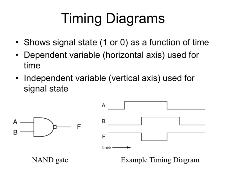
Timing Diagrams • Shows signal state (1 or 0) as a function of time • Dependent variable (horizontal axis) used for time • Independent variable (vertical axis) used for signal state NAND gate Example Timing Diagram Device Models • Model: An arbitrarily defined set of characteristics used to describe the operation of a device. inverter tpHL Idealized model tpLH Model with gate delays Propagation Delays • Present in all digital devices • Prop delays vary based on – device type – device family – device operating conditions • Rising signal delays (tpLH) and falling signal delay times (tpHL) are usually different for a given device Timing Diagram Annotation • Draw reader’s attention to important conditions in circuit • Help them find the “trees” instead of getting overwhelmed with the “forest” Timing Diagram Annotation • Draw reader’s attention to important conditions in circuit • All timing diagrams should be annotated! arrows show simple cause and effect relationship a more complex circuit •Did we mention that… ……All timing diagrams should be annotated!? Circuit Simulation • Allows for testing a design before actual circuit implementation • Simulation represents a “best guess” of how the circuit will operate • Accuracy of simulation compared to actual circuit based on quality of models used • B2 Spice A/D Lite used for Experiment 4 Available for FREE: http://www.beigebag.com/adv4_lite.htm Glitches • Unwanted momentary error conditions in circuit Glitches • Glitches have many causes – cross talk – EMI (Electro-Magnetic Interference) – switching noise – Logic hazards in circuit design • Experiment 4 glitches caused by device propagation delays in circuit elements Glitches: Experiment 4 • Caused by static logic hazards – change in single input variable causes unexpected change in output Only Input A changes 10 1 BC F(A,B,C) = F(0,1,1) = 1 00 01 11 10 A 0 0 1 1 0 1 0 0 1 1 1 F(A,B,C) = F(1,1,1) = 1 “Static” – F stays @ 1 Glitches: Experiment 4 • Glitches prevented by including additional cover terms in K-map Example shown in Experiment 4: BC 00 01 11 10 0 0 1 1 0 1 0 0 1 1 A “Logic Hazard Cover Term” Experiment 4 Procedure Overview • • • • B2 Spice A/D Lite tutorial (DONE!!?) Ring Oscillator analysis Static-1 logic hazard detection & removal Static-0 logic hazard detection & removal Ring Oscillator Include output ports for every gate output …so you can observe how the circuit operates How Do You Choose What Values (1/0) to Apply to Your Inputs To Provoke a Possible Glitch?? • How many inputs should change simultaneously to induce a glitch? • How can we determine which input signal levels may cause a glitch? • Which direction should you change your one input signal? 1 0 or 0 1? For Next Week: • Note which Logic Analyzer Model is at your station (HP 1651A or HP 1663) • Review the tutorial: “An Intuitive Description of the Logic Analyzer” • Read Experiment #5 to prepare for using the Logic Analyzer and the Xilinx Tools – Be sure to download and review the correct Experiment #5 version for YOUR particular model of Logic Analyzer • There are 2 different versions – one for each LA model.


