How Do We Control Material Processes at the Level of Electrons? (V
advertisement

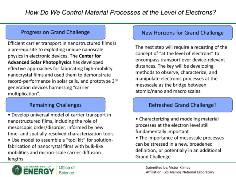
How Do We Control Material Processes at the Level of Electrons? Progress on Grand Challenge Efficient carrier transport in nanostructured films is a prerequisite to exploiting unique nanoscale physics in electronic devices. The Center for Advanced Solar Photophysics has developed effective approaches for fabricating high-mobility nanocrystal films and used them to demonstrate record-performance in solar cells, and prototype 3rd generation devices harnessing “carrier multiplication”. Remaining Challenges • Develop universal model of carrier transport in nanostructured films, including the role of mesoscopic order/disorder, informed by new time- and spatially-resolved characterization tools • Use model to assemble a “tool kit” for solutionfabrication of nanocrystal films with bulk-like mobilities and micron-scale carrier diffusion lengths. New Horizons for Grand Challenge The next step will require a recasting of the concept of “at the level of electrons” to encompass transport over device-relevant distances. The key will be developing methods to observe, characterize, and manipulate electronic processes at the mesoscale as the bridge between atomic/nano and macro scales. Refreshed Grand Challenge? • Characterizing and modeling material processes at the electron level still fundamentally important • The importance of mesoscale processes can be stressed in a new, broadened definition, or potentially in an additional Grand Challenge. Submitted by: Victor Klimov Affiliation: Los Alamos National Laboratory 1 Carrier transport in quantum dot films: From fundamental understanding to optimization in real devices Scientific Achievement (a) Efficient carrier transport through assemblies of quantum dots (QDs) is a prerequisite to harnessing their unique physics in electronic devices. CASP scientists have made numerous direction-setting contributions to the field of conductive QD films in the context of photovoltaics (PVs). First certified QD solar cells: Luther, et al., Adv. Mater. 2010; Gao, et al., Nano Lett. 2011. (b) Mid-gap band in QD films: Nagpal and Klimov, Nat. Commun. 2011; Pal, et al., Adv. Funct. Mater. 2012. Significance and Impact (c) Solar cell with EQE > 100%: Semonin, et al., Science 2012. ALD infilling: Ihly, et al., ACS Nano 2011; Liu, et al., Nano Lett. 2011 and 2013. (d) By bringing together diverse expertise and capabilities, CASP can systematically attack the problem of carrier transport in QD films at multiple levels, from fundamental optical studies, through rational design and assembly of coupled QD films, all the way to fabrication of real PV devices. As a result, CASP has both achieved important firsts in QD solar cells, and contributed vitally to the understanding of transport physics that will enable the next performance breakthroughs. Notable Accomplishments (at left) a) First officially performance-certified “Quantum Dot Solar Cell” b) Uncovering the role of mid-gap band in photoconductivity in PbS QD (e) films and detectors c) First thin-film solar cell with >100% external quantum efficiency (EQE) Transport in through carrier multiplication mesoscopically ordered QD films: d) Record high carrier mobilities and stability in “all inorganic” QD films M. Law, et al., in through atomic-layer deposition (ALD) infilling review. e) Fabrication and studies of transport in QD films with mesoscale ordering


