quiz2_05s-soln
advertisement
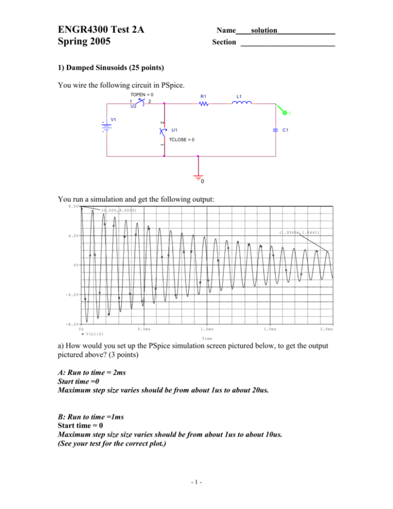
ENGR4300 Test 2A Spring 2005 Name____solution_______________ Section _____________________ 1) Damped Sinusoids (25 points) You wire the following circuit in PSpice. TOPEN = 0 1 U2 R1 L1 2 V 2 V1 U1 C1 1 TCLOSE = 0 0 You run a simulation and get the following output: 8.0V (0.000,8.0000) (1.9566m,1.8441) 4.0V 0V -4.0V -8.0V 0s 0.5ms 1.0ms 1.5ms 2.0ms V(L1:2) Time a) How would you set up the PSpice simulation screen pictured below, to get the output pictured above? (3 points) A: Run to time = 2ms Start time =0 Maximum step size varies should be from about 1us to about 20us. B: Run to time =1ms Start time = 0 Maximum step size size varies should be from about 1us to about 10us. (See your test for the correct plot.) -1- ENGR4300 Test 2A Spring 2005 Name____solution_______________ Section _____________________ b) Using the output pictured, determine the damping constant, , of the circuit. (3 points) A: (t0,V0) = (0ms,8V) (t1,V1)=(1.96ms,1.84V) ln(1.84/8) = - (1.96m-0m) = 749.8/s B: (t0,V0) = (0ms,8V) (t1,V1)=(0.99ms,1.1V) ln(1.1/8) = - (0.99m-0m) B: = 2004/s c) What is the resonant frequency of the circuit in Hertz? (3 points) A: f = 22 cycles/1.96ms = 11.22K Hz A: f = 6 cycles/0.98ms = 6060 Hz d) Write an expression in the form v(t ) Ae points) t cos( 0 t ) for the output signal. (3 A: = 2f = 70.5K rad/sec v(t ) 8Ve 749.8t cos(70.5K t ) B: = 2f = 38.08K rad/sec v(t ) 8Ve 2004t cos(38.08K t ) e) Use the general equations for capacitor and inductor behavior (located on the crib sheet for quiz 1), to describe what is happening in this circuit. What is causing the voltage to behave like a damped sinusoid? (5 points) The equation for the capacitor is I C C VL L dVC . The equation for the inductor is dt dI L . The 8 volt source places a charge on the capacitor at time t=0. Then the dt circuit is disconnected from the source and is allowed to oscillate on its own. The capacitor begins to discharge into the rest of the circuit and the voltage across it changes. The current, Ic, caused by the changing voltage of the capacitor (dVc/dt) starts to flow through the inductor. (This is also IL because the circuit is in series.) The changing current in the inductor (dIL/dt) induces a voltage, VL. This changing voltage causes the capacitor to change up again. The process continues. During each cycle some of the energy in the circuit is dissipated by the resistance of the resistor and this causes the signal to decay and eventually disappear. -2- ENGR4300 Test 2A Spring 2005 Name____solution_______________ Section _____________________ f) The differential equation that governs the behavior of a damped sinusoid is given by d 2V dV 2 02V 0 . In a simple RLC circuit like the one in this question, the 2 dt dt 1 angular resonant frequency of the circuit, 0, is given by 0 and the decay LC R constant, , is given by . In the circuit above, the value of the resistor, R1, is 30 2L ohms. What are the values of the capacitor, C1, and the inductor, L1? (6 points) A: 0 R 749.8 = (30)/(2L) L=30/(2)(749.2) = 20mH 2L 1 70.5K=1/sqrt(20m×C) C=1/(L2)=1/(20m×70.5K2) = 0.01F LC B: R1=40 ohms R 2004 = (40)/(2L) L=40/(2)(2004) = 10mH 2L 0 1 38.08K=1/sqrt(10m×C) C=1/(L 2)=1/(10m×38.08K2) = 0.083uF LC g) You want the damping constant of the circuit to be double what it is now. What new value of L1 would choose to make this occur? (2 points) A: L=30/(2)(2)(749.2) = 10mH B: You want damping constant to be ½ of what it is now. L=40/(2)(1/2)(2004)= 20mH -3- ENGR4300 Test 2A Spring 2005 Name____solution_______________ Section _____________________ 2) Thevenin Equivalent Sources (25 points) Part A You build the circuit pictured below R1 R2 R3 R5 A V1 R4 B 0 Test A: Given: R1=30 ohms, R2=2K ohms, R3 = 3K ohms, R4=2K ohms and R5=1K ohms. Given: V1=6V Test B: Given: R1=40 ohms, R2=3K ohms, R3 = 4K ohms, R4=3K ohms and R5=1K ohms. Given: V1=8V a) Find the Thevenin Equivalent voltage, Vth, of this circuit between point A and point B. (6 points) A: Vth = VR4 = V1(R4)/(R1+R2+R3+R4) = 1.707V B: Vth = VR4 = V1(R4)/(R1+R2+R3+R4)=2.390V b) Find the Thevenin Equivalent Resistance, Rth, of this circuit between point A and point B. (6 points) A: Rth = R5 + (R1+R2+R3)//R4 R1+R2+R3=5030 R123//R4 = (5030)(2000)/(5030+2000)=1431 Rth = 1000+1431 = 2431 ohms B: Rth = R5 + (R1+R2+R3)//R4 R1+R2+R3=7040 R123//R4 = (5030)(2000)/(5030+2000)=2103.6 Rth = 1000+1431 = 3103.6 ohms -4- ENGR4300 Test 2A Spring 2005 Name____solution_______________ Section _____________________ c) Redraw the Thevenin equivalent model of the circuit (2 points). d) If you place a 2K ohm load on the circuit, what will the output voltage be between A and B? (2 points) A: Vout =(2000/4431)1.707 = 0.770V B: Vout = =(3000/3104)2.39 = 1.175V e) What is the current through the 2K ohm load resistor from d? (2 points) A: I=V/R I=0.770/2K = 0.385mA B: The load is 3k ohms. I=V/R I=1.175/3K = 0.392mA -5- ENGR4300 Test 2A Spring 2005 Name____solution_______________ Section _____________________ Part B You place a voltage follower into this circuit between A and B, as pictured below. 0 U1 3 + 7 R2 V+ R1 15 V2 R3 OS2 2 A R4 - uA741 OS1 6 1 V3 4 V1 V- OUT R5 5 15 0 B 0 Test A: Given: R1=30 ohms, R2=2K ohms, R3 = 3K ohms, R4=2K ohms and R5=1K ohms. Given: V1=6V Given: R6 is the load of 2K ohms Test B: Given: R1=40 ohms, R2=3K ohms, R3 = 4K ohms, R4=3K ohms and R5=1K ohms. Given: V1=8V Given: R6 is the load of 3K ohms a) What does the voltage follower do in this circuit? (2 points) The voltage follower isolates the circuit we modeled from the load R6. This means that whatever voltage the circuit puts out between A and B will be transferred to R6 without being influenced by the value of R6. b) What is the voltage output between A and B for this circuit now? (3 points) The voltage between A and B will always be the Thevenin voltage for the circuit because the buffer looks like an infinite impedance to it. Since an infinite impedance is much much bigger than Rth, it will not influence the circuit. Therefore, A: VAB = Vth = 1.707V B: VAB = Vth =2.39V c) What is the current though the load resistor, R6? (2 points) A: I=V/R I=1.707/2K = 0.854mA B: I=V/R I=2.39/3K = 0.797mA -6- R6 ENGR4300 Test 2A Spring 2005 Name____solution_______________ Section _____________________ 3) Op Amp Applications – Digital to Analog Conversion (25 points) One family of digital logic we’ll learn about later in the course uses signals that switch discretely between zero and +5V, corresponding to logic levels of 0 (low) and 1 (high), respectively. Here is a chart of the binary numbers from 1 to 16, their decimal equivalents, and corresponding voltage inputs: Decimal Value Binary Value x2^3 x2^2 x2^1 x2^0 0 0 0 0 0 0 0 1 0 0 1 0 0 0 1 1 0 1 0 0 0 1 0 1 0 1 1 0 0 1 1 1 1 0 0 0 1 0 0 1 1 0 1 0 1 0 1 1 1 1 0 0 1 1 0 1 1 1 1 0 1 1 1 1 0 1 2 3 4 5 6 7 8 9 10 11 12 13 14 15 c Corresponding Voltage Inputs Va Vb Vc Vd 0 0 0 0 0 0 0 5 0 0 5 0 0 0 5 5 0 5 0 0 0 5 0 5 0 5 5 0 0 5 5 5 5 0 0 0 5 0 0 5 5 0 5 0 5 0 5 5 5 5 0 0 5 5 0 5 5 5 5 0 5 5 5 5 The following op amp circuit is configured as a digital to analog (D/A) converter. Our D/A converter shown here is a three bit converter: logic voltages at V1, V2, and V3 generate an output voltage at Vout. V1 is the lowest order bit corresponding to Vd (in the chart), V2 corresponds to Vc, and V3 corresponds to Vb. R4 R6 15Vdc V1 R1 U1 7 3 V2 + - uA741 V3 V+ OS2 OUT R2 2 15Vdc 0 4 OS1 V- 0 U2 7 5 3 R5 + 6 V+ OS2 OUT 1 2 - uA741 4 OS1 V- 5 6 Vout 1 R7 R3 15Vdc 0 15Vdc 0 0 Component values for the circuit shown are as follows: R4 = 5k, R5 = 20k, R6 = 10k, R7 = 10Meg ohms. Values R1, R2, and R3 will be determined by you in part b of this question. -7- ENGR4300 Test 2A Spring 2005 Name____solution_______________ Section _____________________ Test B: Component values for the circuit shown are as follows: R4 = 4k, R5 = 40k, R6 = 10k, R7 = 1Meg ohms. Values R1, R2, and R3 will be determined by you in part b of this question. a. Given the D/A circuit on the previous page, about what is the maximum voltage rounded to the nearest 0.5 volts (e.g. 1.0V, 1.5V, 2.0V,…) that the circuit should generate at Vout when it is acting correctly as a D/A converter? Describe your reasoning for this answer and show all equations or calculations used to arrive at this answer. (3 points) The maximum output for a three bit binary number is 111. This corresponds to the decimal number 7, so the circuit should output a maximum of 7 volts. There is another answer to this question. If you assumed that the output of the first opamp could put out -15 (or anything from -15 to -13), and used the gain of the second opamp, (-10k/20k), to predict that the circuit could deliver a maximum of 7.5 volts at the output, then this is right too. b. The D/A should generate output voltages between 0V for a binary input of 000 to the full scale value you determined in part A when a binary input of 111 is present with a proportional increase in voltage as the binary value increases from 000 to 111. Determine the resistor values R1, R2, and R3 that achieve this in the circuit. (12 points) A: Vx=(-R4)[(VD/R1)+(VC/R2)+(VB/R3)] Vout = (-R6/R5)Vx Vout=(R4*R6/R5)[(VD/R1)+(VC/R2)+(VB/R3)] (R4*R6/R5)=(5K*10K)/20K=2.5K Vout 1 2 4 VB (V3) 0 0 5V VC(V2) VD(V1) plug in solve 0 5V 0 R1=12.5K R2=6.25K R3=3.125K 5V 0 0 2.5K(5/R1)=1 2.5K(5/R2)=2 2.5K(5/R3)=4 A: R1 = 12500 ohms R2 = 6250 ohms R3 = 3125 ohms -8- ENGR4300 Test 2A Spring 2005 Name____solution_______________ Section _____________________ B: (R4*R6/R5)=(4K*10K)/40K=1K Vout 1 2 4 VB (V3) 0 0 5V VC(V2) VD(V1) plug in solve 0 5V 0 R1=5K R2=2.5K R3=1.25K 5V 0 0 1K(5/R1)=1 1K(5/R2)=2 1K(5/R3)=4 B: R1 = 5000 ohms R2 = 2500 ohms R3 = 1250ohms c. Show the output voltage at Vout will give the correct decimal value for the following two binary input combinations: ( 7 points). A: 100: Vout=(2.5K)[(0/12500)+(0/6250)+(5/3125)] = 4V ? 4V = 4V 011: Vout=(2.5K)[(5/12500)+(5/6250)+(0/3125)] = 3V ? 3V = 3V B: 010: Vout=(1K)[(0/5000)+(5/2500)+(5/1250)] = 2V ? 2V = 2V 101: Vout=(1K)[(5/5000)+(0/2500)+(5/1250)] = 5V ? 5V = 5V d. The second op amp (rightmost in the schematic shown) performs two primary functions in this circuit. One of these functions could instead be integrated into the first op amp circuit by using a different selection of resistor values. What function does this op amp perform that cannot be integrated with the first op amp? (A one sentence answer is worth 3 points.) The second op-amp circuit inverts the signal and changes the gain. We could alter the gain to whatever we want with the adder, but we cannot do the inversion. Invert the signal. -9- ENGR4300 Test 2A Spring 2005 Name____solution_______________ Section _____________________ 4) Op Amp Analysis (25 points) Part A Given the op-amp circuit below: R5 15Vdc V1 R1 3 V2 0 U1 7 + V+ OS2 OUT R2 2 - uA741 4 OS1 V- 5 Vout 6 1 15Vdc R3 R4 0 Test A: R1 = R2 = 2k, R3 = R4 = 6k, R5 = 3k Test B: R1 = R2 = 1k, R3 = R4 = 8k, R5 = 4k a. What op-amp circuit given on your crib sheet does this circuit most closely represent? (Hint: disregard specific resistor values) (2 points) Difference (differential) amplifier b. What are the golden rules of op amp analysis? (2 points) 1) V+ = V2) I+ = I- = 0 - 10 - ENGR4300 Test 2A Spring 2005 Name____solution_______________ Section _____________________ c. Find an expression for Vout in terms of V1, V2 and resistor values R1, R2, R3, R4, and R5 (do not substitute actual resistor values) (12 points) Let R34 = R3*R4/(R3+R4) : i V2 VB VB Vout R2 R34 : VA R5 V1 R1 R5 V2 Vout R2 R34 solve for VB : VB 1 1 R2 R34 V A VB : R34V2 R2Vout R2 R34 VB R34 R2 R2 R34 VB R34 R2 V2 Vout R34 R2 R34 R2 R5 R34 R2 V1 V2 Vout R1 R5 R34 R2 R34 R2 R5 R34 R2 Vout V1 V2 R34 R2 R1 R5 R34 R2 Vout R34 R34 R2 R5 R R2 R34 V1 34 V2 R2 R1 R5 R2 R34 R2 R3 R4 Vout R3 R4 R3 R4 R3 R4 R2 R R4 R5 R R4 3 V1 3 V2 R2 R1 R5 R2 That is as far as I’m going with this one. If they reduce further that is good, but this is ok. d. Substitute resistor values in this equation and write the equation for Vout in terms of V1 and V2 input signals. (3 points) R34 A: R3 R4 6k 6k 3k 2k 3k 3k 3 3k Vout V1 V2 (V1 V2 ) R3 R4 6k 6k 2k 2k 3k 2k 2 3 Vout (V1 V2 ) 2 B: R34 R3 R4 8k 8k 4k 1k 4k 4k 4k Vout V1 V2 4(V1 V2 ) R3 R4 8k 8k 1k 1k 4k 1k Vout 4(V1 V2 ) - 11 - ENGR4300 Test 2A Spring 2005 Name____solution_______________ Section _____________________ Part B What if R4 is replaced by a 10uF capacitor and V1 is grounded, as shown below? a. What function is this circuit designed to perform? (2 points) This circuit does integration. It is a Miller integrator. b. Write the transfer function Vout/V2 for this circuit (2 points) R3 Zf V j R3C 1 R3 6k 6k A: out V2 Z in R2 j R2 R3C R2 j 2k 6k10 2k j 120 2k R3 Zf V j R3C 1 R3 8k 8k B: out V2 Z in R2 j R2 R3C R2 j 1k 8k10 1k j 80 1k c. Over about what frequency range is the desired function of the circuit reliably performed? [You can assume that the operation is being performed even when the output amplitude is very small.] (2 points) 1 1 = 2.65 2R3C 2 6k10 Hz. I am going to choose 5 times 2 Hz since that worked well on the quiz we went over in class. Therefore, this circuit works as an integrator at frequencies above 13 Hz. (Anything between 5 and 27 hertz is ok.) A: This circuit works at frequencies much greater than fc - 12 - ENGR4300 Test 2A Spring 2005 Name____solution_______________ Section _____________________ 1 1 = 2 Hz. 2R3C 2 8k10 I am going to choose 5 times 2 Hz since that worked well on the quiz we went over in class. Therefore, this circuit works as an integrator at frequencies above 10 Hz. (Anything between 4 and 20 hertz is ok.) B: This circuit works at frequencies much greater than fc - 13 -
