Optical Interconnects using Optical Far- and Near
advertisement
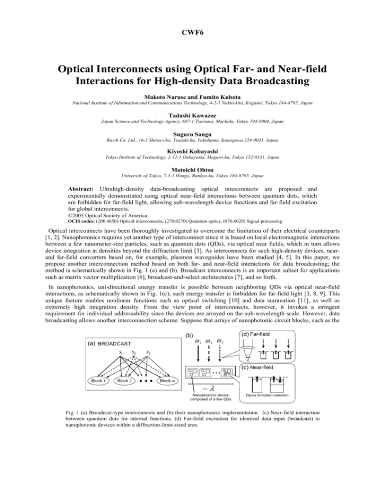
CWF6 Optical Interconnects using Optical Far- and Near-field Interactions for High-density Data Broadcasting Makoto Naruse and Fumito Kubota National Institute of Information and Communications Technology, 4-2-1 Nukui-kita, Koganei, Tokyo 184-8795, Japan Tadashi Kawazoe Japan Science and Technology Agency, 687-1 Tsuruma, Machida, Tokyo 194-0004, Japan Suguru Sangu Ricoh Co. Ltd., 16-1 Shinei-cho, Tsuzuki-ku, Yokohama, Kanagawa 224-0035, Japan Kiyoshi Kobayashi Tokyo Institute of Technology, 2-12-1 Ookayama, Meguro-ku, Tokyo 152-8551, Japan Motoichi Ohtsu University of Tokyo, 7-3-1 Hongo, Bunkyo-ku, Tokyo 184-8795, Japan Abstract: Ultrahigh-density data-broadcasting optical interconnects are proposed and experimentally demonstrated using optical near-field interactions between quantum dots, which are forbidden for far-field light, allowing sub-wavelength device functions and far-field excitation for global interconnects. 2005 Optical Society of America OCIS codes: (200.4650) Optical interconnects, (270.0270) Quantum optics, (070.6020) Signal processing Optical interconnects have been thoroughly investigated to overcome the limitation of their electrical counterparts [1, 2]. Nanophotonics requires yet another type of interconnect since it is based on local electromagnetic interactions between a few nanometer-size particles, such as quantum dots (QDs), via optical near fields, which in turn allows device integration at densities beyond the diffraction limit [3]. As interconnects for such high-density devices, nearand far-field converters based on, for example, plasmon waveguides have been studied [4, 5]. In this paper, we propose another interconnection method based on both far- and near-field interactions for data broadcasting; the method is schematically shown in Fig. 1 (a) and (b). Broadcast interconnects is an important subset for applications such as matrix vector multiplication [6], broadcast-and-select architectures [7], and so forth. In nanophotonics, uni-directional energy transfer is possible between neighboring QDs via optical near-field interactions, as schematically shown in Fig. 1(c); such energy transfer is forbidden for far-field light [3, 8, 9]. This unique feature enables nonlinear functions such as optical switching [10] and data summation [11], as well as extremely high integration density. From the view point of interconnects, however, it invokes a stringent requirement for individual addressability since the devices are arrayed on the sub-wavelength scale. However, data broadcasting allows another interconnection scheme. Suppose that arrays of nanophotonic circuit blocks, such as the (b) (a) BROADCAST s1 s2 ϖ1 ϖ 2 ϖ 3 (d) Far-field s2 λ (c) Near-field Block 1 Block 2 Block m ~λ Nanophotonic device composed of a few QDs Dipole forbidden transition Fig. 1 (a) Broadcast-type interconnects and (b) their nanophotonics implementation. (c) Near-field interaction between quantum dots for internal functions. (d) Far-field excitation for identical data input (broadcast) to nanophotonic devices within a diffraction-limit-sized area. CWF6 nanophotonic switches described later, are distributed within an area whose size is comparable to the wavelength, as shown in Fig. 1(d). Here, for broadcasting, multiple nanophotonic input QDs simultaneously accept identical input data carried by diffraction-limited far-field light by tuning the optical frequency so that the light is coupled to dipole-allowed energy sublevels, as describe below. In a frequency multiplexing sense, this interconnection method is similar to multi-wavelength chip-scale interconnects [12]. However, known methods require a physical space comparable to the number of diffraction-limited input channels due to wavelength demultiplexing, whereas in our proposed scheme, the device arrays are integrated on the sub-wavelength scale, and multiple frequencies are multiplexed in the far-field light supplied to the device. Here we explain the near- and far-field coupling mentioned above based on a model assuming CuCl QDs, which are later employed in experiments; these QDs are also used to demonstrate the principles of nanophotonic switching [6] and summation [7]. The potential barrier of CuCl QDs in a NaCl crystal can be regarded as infinitely high, and the energy eigenvalues for the quantized Z3 exciton energy level (nx,ny,nz) in a CuCl QD with side of length L are given by E( nx ,n y ,nz ) = E B + h 2π 2 (n x2 + n y2 + n z2 ) 2M ( L − a B ) 2 (1) where EB is the bulk energy of the Z3 exciton, M is the translational mass of the exciton, aB is its Bohr radius, nx, ny, and nz are quantum numbers (nx, ny, nz=1,2,3,…), and a=L-aB corresponds to an effective side length found after considering the dead layer correction. The exciton energy levels with even quantum numbers are dipole-forbidden states [13]. The optical near-field interaction, however, is allowed for such energy levels. According to (1) there exists a resonance between the quantized exciton energy sublevel of quantum number (1,1,1) for the QD with effective side length a and that of quantum number (2,1,1) for the QD with effective side length 2a . (For simplicity, we refer to the QDs with effective side lengths a and 2a as "QD a" and "QD 2a ", respectively.) Therefore, energy transfer between QD a and QD 2a occurs, which is forbidden for far-field light; this plays a critical role in the internal operation of nanophotonic devices. Here, we notice that the input energy level for the QDs, that is, the (1,1,1)-level, can also couple to the far-field excitation. We utilized this fact for data broadcasting. One of the design restrictions is that energy-sublevels for input channels do not overlap with those for outputs. Also, if there are QDs internally used for near-field coupling, dipole-allowed energy sublevels for those QDs cannot be used for input channels since the inputs are provided by far-field light, which may lead to misbehavior of internal near-field interactions if resonant levels exist. Therefore, frequency partitioning among the input, internal, and output channels is important; this is schematically shown in Fig. 2(a). Fig. 2(b) shows a diagram for illustrating frequency partitioning, where the horizontal axis shows QD size and the vertical axis shows energy sublevels. The 3-digit sets in the diagram are the principle quantum numbers of the QDs. As an example, we used a nanophotonic switch (2-input AND gate) composed of three QDs with a size ratio of 1 : 2 : 2 . The details of the switching principle are shown in reference [10]. The two input channels are assigned to QD a and QD 2a, and the output appears from QD 2a . Here, multiple input dots QD a and QD 2a can accept identical input data via far-field light for broadcasting purposes. Also, adding more optical switches means adding different size dots so that the corresponding far-field resonant frequencies do not overlap with the other channels. For instance by multiplying the scale of the QDs by a natural number, such as 2 2a , 4a , and 4 2a , the number of Quantum dot size (b) a ϖ i ,1 ,ϖ i , 2 ,L Internal ϖ n ,1 ,ϖ n , 2 , L Output ϖ o ,1 ,ϖ o, 2 , L Frequency (a) Input Frequency ϖ i ,1 ϖ i,5 ϖ 0 ,1 ϖ 0 ,6 ϖ i, 2 ϖ i,6 ϖ i,3 ϖ 0,2 ϖ i, 4 2a 2a 2 2a 4a 4 2a (1,1,1) (2,1,1) (2,2,2) (4,2,2) (4,4,4) (8,4,4) 4 / 3a , 8 / 3a , (2,2,1) (4,1,1) (4,4,2) (8,2,2) (1,1,1) (2,1,1) (2,2,2) (4,2,2) (4,4,4) (2,2,1) (4,1,1) (4,4,2) (1,1,1) (2,1,1) (2,2,2) (4,2,2) (2,2,1) (4,1,1) (1,1,1) (2,1,1) (2,2,2) (2,2,1) (1,1,1) (2,1,1) 16 / 3a (1,1,1) Fig. 2 (a) Frequency partitioning for external and internal nanophotonic operations. (b) Frequency-diagram for multiple implementations of 3-dot nanophotonic switches. CWF6 channels increases. More dense integration is also possible by appropriately configuring the size of the QDs. As an example, consider a QD whose size is 4 / 3a . The (1,1,1)-level in this QD 4 / 3a can couple to the far-field excitation. It should be noted that this particular energy level is equal to the (2,2,1)-level in QD 2a, which is an already-used input channel; however, the far-field excitation cannot couple to QD 2a since the (2,2,1)-level in QD 2a is a dipole-forbidden energy sub-level. Therefore, a QD trio composed of 4 / 3a , 8 / 3a , and 16 / 3a can make up another optical switch, while not interfering with other channels even though all of the input light is irradiated in the same area whose size is determined by the diffraction limit of light. The size of these QDs should be approximately an integer multiple of half the lattice constant. To verify the broadcasting method, we performed the following experiments using CuCl QDs which were inhomogeneously distributed in a NaCl matrix at a temperature of 22 K. To operate a 3-dot nanophotonic switch (2input AND gate) in the device, we irradiated at most two input light beams (IN1 and IN2) via far-field light. When both inputs exist, an output signal is obtained through optical near-field interactions from the positions where the switches exist, as described above. In the experiment, IN1 and IN2 were assigned to 325 nm and 384.7 nm, respectively: They were irradiated over the entire sample (global irradiation). The spatial intensity distribution of the output, at 382.6 nm, was measured by scanning a near-field fiber probe within an area of 1 µm × 1 µm, as shown in Fig. 3. In Fig. 3(a), only IN1 was applied to the sample, whereas in Fig. 3(b) both inputs were irradiated. Here, note the regions marked by , , and . In those regions, the output signal levels were respectively low and high in Fig. 3(a) and (b), which indicates that multiple AND gates were integrated at densities beyond the diffraction limit of light while input data was globally irradiated, that is to say, using broadcast interconnects, by far-field light. In summary, broadcast interconnects for nanophotonic devices are proposed and experimentally demonstrated using far- and near-field interactions. Combining this broadcasting mechanism with switching [10] and summation [11] will allow the development of nano-scale integration of optical parallel processing devices, which have conventionally resulted in bulky systems. Reference [1] D. A. B. Miller, “Rationale and Challenges for Optical Interconnects to Electronic Chips,” Proc. IEEE, 88, 728-749 (2000). [2] N. McArdle, M. Naruse, H. Toyoda, Y. Kobayashi, and M. Ishikawa, “Reconfigurable Optical Interconnections for Parallel Computing,” Proc. IEEE 88, 829-837 (2000). [3] M. Ohtsu, K. Kobayashi, T. Kawazoe, S. Sangu, and T. Yatsui, “Nanophotonics: design, fabrication, and operation of nanometric devices using optical near fields,” IEEE J. Select. Topics Quantum Electron. 8, 839-862 (2002). [4] T. Yatsui, M. Kourogi, and M. Ohtsu, “Plasmon waveguide for optical far/near-field conversion,” Appl. Phys. Lett. 79, 4583-4585 (2001). [5] J. Takahara, Y. Suguru, T. Hiroaki, A. Morimoto, and T. Kobayashi, “Guiding of a one-dimensional optical beam with nanometer diameter,” Opt. Lett. 22, 475-477 (1997). [6] P. S. Guilfoyle and D. S. McCallum, “High-speed low-energy digital optical processors,” Opt. Eng. 35, 436-442 (1996). [7] B. Li, Y.Qin, X. Cao, and K. M. Sivalingam, “Photonic packet switching: Architecture and performance,” Optical Networks Magazine 2, 2739 (2001). [8] K. Kobayashi and M. Ohtsu, “Quantum theoretical approach to a near-field optical system,” J. Microsc. 194, 249-254 (1999). [9] T. Kawazoe, K. Kobayashi, J. Lim, Y. Narita, and M. Ohtsu, “Direct Observation of Optically Forbidden Energy Transfer between CuCl Quantum Cubes via Near-Field Optical Spectroscopy”, Phys. Rev. Lett. 88, 067404-1-4 (2002). [10] T. Kawazoe, K. Kobayashi, S. Sangu, and M. Ohtsu, “Demonstration of a nanophotonic switching operation by optical near-field energy transfer,” Appl. Phys. Lett. 82, 2957-2959 (2003). [11] M. Naruse, T. Miyazaki, F. Kubota, T. Kawazoe, K. Kobayashi, S. Sangu, and M. Ohtsu, “Nanometric summation architecture using optical near-field interaction between quantum dots,” Opt. Lett., in press. [12] E. A. De Souza, M. C. Nuss, W. H. Knox, and D. A. B. Miller, “Wavelength-division multiplexing with femtosecond pulses,” Opt. Lett. 20, 1166-1168 (1995). [13] Z. K. Tang, A. Yanase, T. Yasui, Y. Segawa, and K. Cho, “Optical selection rule and oscillator strength of confined exciton system in CuCl thin films,” Phys. Rev. Lett. 71, 1431-1434 (1993). 1µm (b) IN1: 325nm IN2: none IN1: 325nm IN2: 384.7nm 1µm (a) Fig. 3 Experimental results. Spatial intensity distribution of the output (382.6nm) of AND gates. (a) Output level: low ( 1 AND 0 = 0), and (b) output level: high (1 AND 1 = 1)
