BT.656 Video Interface for ICs
®
Application Note
July 2002
Introduction
AN9728.2
Because of its capabilities, a TTL compatible version of the
parallel interface is now being used as a chip-to-chip interface for video ICs.
When ITU-R BT.601, formally CCIR-601, was developed
(which defined the YCbCr color space, the 4:2:2 YCbCr
sampling organization, and sampling resolutions), it was
soon followed by ITU-R BT.656 (formally CCIR-656).
YCbCr Video Stream
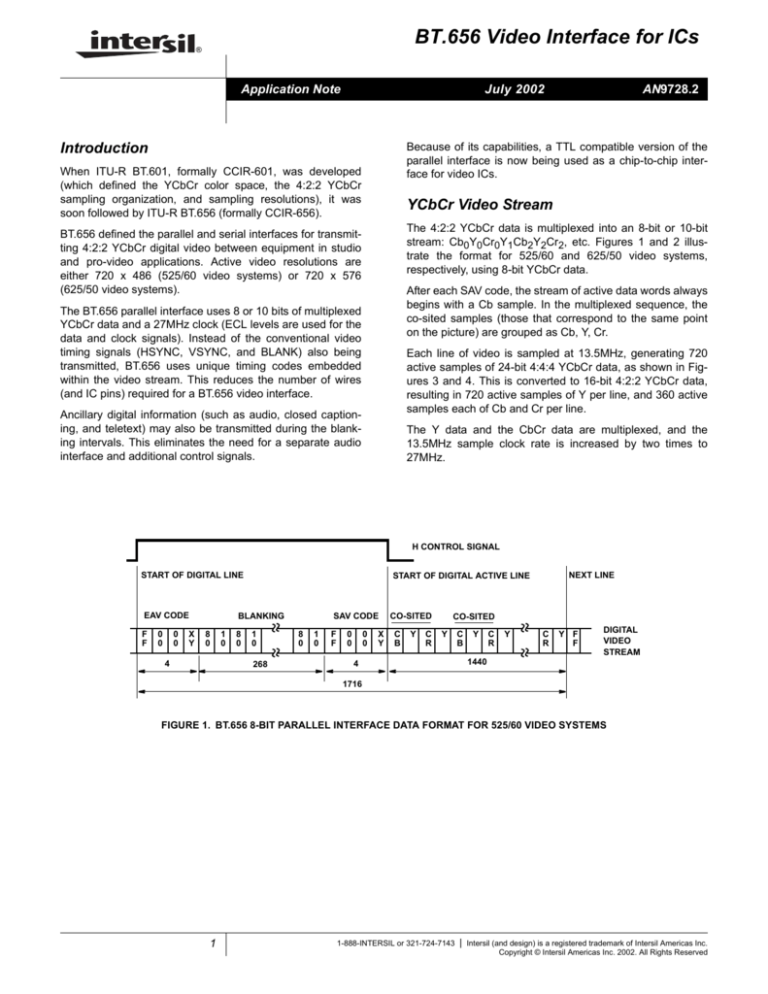
The 4:2:2 YCbCr data is multiplexed into an 8-bit or 10-bit
stream: Cb0Y0Cr0Y1Cb2Y2Cr2, etc. Figures 1 and 2 illustrate the format for 525/60 and 625/50 video systems,
respectively, using 8-bit YCbCr data.
BT.656 defined the parallel and serial interfaces for transmitting 4:2:2 YCbCr digital video between equipment in studio
and pro-video applications. Active video resolutions are
either 720 x 486 (525/60 video systems) or 720 x 576
(625/50 video systems).
After each SAV code, the stream of active data words always
begins with a Cb sample. In the multiplexed sequence, the
co-sited samples (those that correspond to the same point
on the picture) are grouped as Cb, Y, Cr.
The BT.656 parallel interface uses 8 or 10 bits of multiplexed
YCbCr data and a 27MHz clock (ECL levels are used for the
data and clock signals). Instead of the conventional video
timing signals (HSYNC, VSYNC, and BLANK) also being
transmitted, BT.656 uses unique timing codes embedded
within the video stream. This reduces the number of wires
(and IC pins) required for a BT.656 video interface.
Each line of video is sampled at 13.5MHz, generating 720
active samples of 24-bit 4:4:4 YCbCr data, as shown in Figures 3 and 4. This is converted to 16-bit 4:2:2 YCbCr data,
resulting in 720 active samples of Y per line, and 360 active
samples each of Cb and Cr per line.
Ancillary digital information (such as audio, closed captioning, and teletext) may also be transmitted during the blanking intervals. This eliminates the need for a separate audio
interface and additional control signals.
The Y data and the CbCr data are multiplexed, and the
13.5MHz sample clock rate is increased by two times to
27MHz.
H CONTROL SIGNAL
START OF DIGITAL LINE
EAV CODE
F
F
0
0
0
0
X
Y
SAV CODE
BLANKING
8
0
4
1
0
8
0
NEXT LINE
START OF DIGITAL ACTIVE LINE
1
0
268
8
0
1
0
F
F
0
0
0
0
X
Y
CO-SITED
C
B
Y
C
R
CO-SITED
Y
C
B
Y
C
R
Y
C
R
Y F
F
DIGITAL
VIDEO
STREAM
1440
4
1716
FIGURE 1. BT.656 8-BIT PARALLEL INTERFACE DATA FORMAT FOR 525/60 VIDEO SYSTEMS
1
1-888-INTERSIL or 321-724-7143
|
Intersil (and design) is a registered trademark of Intersil Americas Inc.
Copyright © Intersil Americas Inc. 2002. All Rights Reserved
Application Note 9728
H CONTROL SIGNAL
START OF DIGITAL LINE
EAV CODE
F
F
0
0
0
0
BLANKING
X
Y
8
0
1
0
8
0
4
NEXT LINE
START OF DIGITAL ACTIVE LINE
1
0
280
SAV CODE
8
0
1
0
F
F
0
0
0
0
X
Y
CO-SITED
C
B
Y
C
R
CO-SITED
Y
C
B
Y
C
R
Y
C
R
Y F
F
DIGITAL
VIDEO
STREAM
1440
4
1728
FIGURE 2. BT.656 8-BIT PARALLEL INTERFACE DATA FORMAT FOR 625/50 VIDEO SYSTEMS
T = 1/13.5MHz
T = 1/13.5MHz
12T
16T
50% SYNC
LEVEL
50% SYNC
LEVEL
DIGITAL
BLANKING
DIGITAL ACTIVE LINE
138T
(720-857)
720T
(0-719)
TOTAL LINE
858T
(0-857)
FIGURE 3. BT.656 HORIZONTAL TIMING RELATIONSHIP FOR
525/60 VIDEO SYSTEMS
SAV and EAV Timing Codes
SAV (start of active video) and EAV (end of active video)
codes are embedded within the YCbCr video stream. They
eliminate the need for the HSYNC, VSYNC, and BLANK timing signals normally used in a video system. The EAV and
SAV sequences are shown in Table 1.
The XY status word, which also indicates whether it is an
SAV or EAV sequence, is defined as:
F = 0 for field 1; F = 1 for field 2
V = 1 during vertical blanking
H = 0 at SAV, H = 1 at EAV
DIGITAL
BLANKING
DIGITAL ACTIVE LINE
144T
(720-863)
720T
(0-719)
TOTAL LINE
864T
(0-863)
FIGURE 4. BT.656 HORIZONTAL TIMING RELATIONSHIP FOR
625/50 VIDEO SYSTEMS
rected (and some multiple bit errors detected) at the
receiver. Although they should always be generated in video
IC interconnect applications, they are usually ignored by the
receiving IC.
BT.656 uses the BT.601 - defined vertical blanking intervals,
as shown in Figures 5 and 6. However, note that active resolutions other than 720 x 486 and 720 x 576 may be supported (effectively cropping the image) by adjusting where
the EAV and SAV codes and vertical blanking intervals
occur.
Square Pixel Variation
A variation using square pixels has been developed,
although not endorsed by the BT.656 standard. Instead of a
27MHz clock, a 24.54MHz clock is used for 525/60 video
systems (640 x 480 active resolution), and a 29.5MHz clock is
used for 625/50 video systems (768 x 576 active resolution).
P3-P0 = protection bits
P3 = V ⊕ H
P2 = F ⊕ H
P1 = F ⊕ V
P0 = F ⊕ V ⊕ H
where ⊕ represents the exclusive-OR function. These protection bits enable single-bit errors to be detected and cor2
Figures 7 and 8 illustrate the data format, Figures 9 and 10
illustrate the horizontal timing relationships, and Figures 11
and 12 show the vertical blanking intervals.
Application Note 9728
TABLE 1. BT.656 EAV AND SAV SEQUENCE
8-BIT DATA
Preamble
Status Word
10-BIT DATA
D9
(MSB)
D8
D7
D6
D5
D4
D3
D2
D1
D0
1
1
1
1
1
1
1
1
1
1
0
0
0
0
0
0
0
0
0
0
0
0
0
0
0
0
0
0
0
0
1
F
V
H
P3
P2
P1
P0
0
0
LINE 1 (V = 1)
LINE 4
BLANKING
FIELD 1
(F = 0)
ODD
LINE 21 (V = 0)
FIELD 1
ACTIVE VIDEO
LINE 264 (V = 1)
LINE 266
BLANKING
FIELD 2
(F = 1)
EVEN
LINE 283 (V = 0)
FIELD 2
ACTIVE VIDEO
LINE
NUMBER
F
V
H
(EAV)
H
(SAV)
1-3
1
1
1
0
4-20
0
1
1
0
21-263
0
0
1
0
264-265
0
1
1
0
266-282
1
1
1
0
283-525
1
0
1
0
H
(EAV)
H
(SAV)
LINE 525 (V = 0)
LINE 3
H=1 H=0
EAV SAV
FIGURE 5. TYPICAL BT.656 VERTICAL BLANKING INTERVALS FOR 525/60 VIDEO SYSTEMS
LINE 1
LINE 1 (V = 1)
BLANKING
LINE 23 (V = 0)
FIELD 1
(F = 0)
ODD
FIELD 1
ACTIVE VIDEO
LINE 311 (V = 1)
LINE 313
BLANKING
LINE 336 (V = 0)
FIELD 2
ACTIVE VIDEO
FIELD 2
(F = 1)
EVEN
LINE
NUMBER
F
V
1-22
0
1
1
0
23-310
0
0
1
0
311-312
0
1
1
0
313-335
1
1
1
0
336-623
1
0
1
0
624-625
1
1
1
0
LINE 624 (V = 1)
BLANKING
LINE 625 (V = 1)
LINE 625
H=1 H=0
EAV SAV
FIGURE 6. TYPICAL BT.656 VERTICAL BLANKING INTERVALS FOR 625/50 VIDEO SYSTEMS
3
Application Note 9728
H CONTROL SIGNAL
START OF DIGITAL LINE
EAV CODE
F
F
0
0
0
0
BLANKING
X
Y
8
0
1
0
8
0
4
NEXT LINE
START OF DIGITAL ACTIVE LINE
1
0
SAV CODE
8
0
1
0
F
F
0
0
0
0
X
Y
CO-SITED
C
B
Y
C
R
CO-SITED
Y
C
B
C
R
Y
C
R
Y F
F
DIGITAL
VIDEO
STREAM
1280
4
272
Y
1560
FIGURE 7. 8-BIT DATA FORMAT FOR SQUARE PIXEL 525/60 VIDEO SYSTEMS
H CONTROL SIGNAL
START OF DIGITAL LINE
EAV CODE
F
F
0
0
0
0
BLANKING
X
Y
8
0
1
0
4
8
0
NEXT LINE
START OF DIGITAL ACTIVE LINE
1
0
344
SAV CODE
8
0
1
0
F
F
0
0
0
0
X
Y
CO-SITED
C
B
Y
C
R
CO-SITED
Y
C
B
Y
C
R
Y
C
R
Y F
F
DIGITAL
VIDEO
STREAM
1536
4
1888
FIGURE 8. 8-BIT DATA FORMAT FOR SQUARE PIXEL 625/50 VIDEO SYSTEMS
T = 1/14.75MHz
T = 1/12.27MHz
23T
23T
50% SYNC
LEVEL
50% SYNC
LEVEL
DIGITAL
BLANKING
DIGITAL ACTIVE LINE
140T
(640-779)
640T
(0-639)
DIGITAL
BLANKING
DIGITAL ACTIVE LINE
176T
(768-943)
768T
(0-767)
TOTAL LINE
TOTAL LINE
944T
(0-943)
780T
(0-779)
FIGURE 9. HORIZONTAL TIMING RELATIONSHIP FOR SQUARE
PIXEL 525/60 VIDEO SYSTEMS
4
FIGURE 10. HORIZONTAL TIMING RELATIONSHIP FOR SQUARE
PIXEL 625/50 VIDEO SYSTEMS
Application Note 9728
LINE 1 (V = 1)
LINE 4
BLANKING
FIELD 1
(F = 0)
ODD
LINE 23 (V = 0)
LINE
NUMBER
F
V
H
(EAV)
H
(SAV)
1-3
1
1
1
0
4-22
0
1
1
0
23-262
0
0
1
0
263-265
0
1
1
0
266-285
1
1
1
0
286-525
1
0
1
0
FIELD 1
ACTIVE VIDEO
LINE 263 (V = 1)
LINE 266
BLANKING
FIELD 2
(F = 1)
EVEN
LINE 286 (V = 0)
FIELD 2
ACTIVE VIDEO
LINE 525 (V = 0)
LINE 3
H=1 H=0
EAV SAV
FIGURE 11. TYPICAL VERTICAL BLANKING INTERVALS FOR SQUARE PIXEL 525/60 VIDEO SYSTEMS
LINE 1
LINE 1 (V = 1)
BLANKING
LINE 23 (V = 0)
FIELD 1
(F = 0)
ODD
LINE
NUMBER
F
V
H
(EAV)
H
(SAV)
1-22
0
1
1
0
23-310
0
0
1
0
311-312
0
1
1
0
313-335
1
1
1
0
336-623
1
0
1
0
624-625
1
1
1
0
FIELD 1
ACTIVE VIDEO
LINE 311 (V = 1)
LINE 313
BLANKING
LINE 336 (V = 0)
FIELD 2
ACTIVE VIDEO
FIELD 2
(F = 1)
EVEN
LINE 624 (V = 1)
BLANKING
LINE 625 (V = 1)
LINE 625
H=1 H=0
EAV SAV
FIGURE 12. TYPICAL VERTICAL BLANKING INTERVALS FOR SQUARE PIXEL 625/50 VIDEO SYSTEMS
Ancillary Data
Ancillary data packets are used to transmit information such
as digital audio, captioning information, and teletext data.
BT.656 discusses ancillary data only in very general terms;
the SMPTE 291M standard goes into much more detail.
single data ID word to indicate the type of ancillary data,
Type 2 (a newer format) uses two words for the data ID.
On scan lines containing active video data, ancillary data
may be transmitted in the time between the EAV sequence
and SAV sequence (horizontal blanking). On blanked scan
lines during the vertical blanking intervals, ancillary data may
be transmitted at any time.
The Data ID word indicates the type of data being sent. The
assignment of most of the Data ID values is controlled by the
ITU and SMPTE to ensure equipment compatibility. A few ID
values are available for user applications that don’t require
registration. Video ICs for the PC multimedia market use
these user-application ID codes to avoid contention with professional video equipment.
There are two types of ancillary data formats, as shown in
Tables 2 and 3. In general, Type 1 (an older format) uses a
5
Data ID (DID)
Application Note 9728
TABLE 2. TYPE 1 ANCILLARY DATA PACKET FORMAT
8-BIT DATA
10-BIT DATA
D9 (MSB)
D8
D7
D6
D5
D4
D3
D2
D1
D0
0
0
0
0
0
0
0
0
0
0
1
1
1
1
1
1
1
1
1
1
1
1
1
1
1
1
1
1
1
1
Data ID
PAR
PAR
Value of 0000 0000 to 1111 1111
Data Block Number
PAR
PAR
Value of 0000 0000 to 1111 1111
Data Word Count
PAR
PAR
Value of 0000 0000 to 1111 1111
Preamble
User Data Word 0
Value of 00 0000 0100 to 11 1111 1011
:
:
User Data Word N
Check Sum
Value of 00 0000 0100 to 11 1111 1011
PAR
Sum of D0–D8 of data ID through last user data word. Preset to all zeros; carry is ignored.
NOTES:
1. PAR = even parity for D0–D7.
2. D8 = inverted value of D8 bit.
3. 8-bit data is transferred using the D2–D9 bits
TABLE 3. TYPE 2 ANCILLARY DATA PACKET FORMAT
8-BIT DATA
10-BIT DATA
D9 (MSB)
D8
D7
D6
D5
D4
D3
D2
D1
D0
0
0
0
0
0
0
0
0
0
0
1
1
1
1
1
1
1
1
1
1
1
1
1
1
1
1
1
1
1
1
Data ID
PAR
PAR
Value of 0000 0000 to 1111 1111
Secondary ID
PAR
PAR
Value of 0000 0000 to 1111 1111
Data Word Count
PAR
PAR
Value of 0000 0000 to 1111 1111
Preamble
User Data Word 0
Value of 00 0000 0100 to 11 1111 1011
:
:
User Data Word N
Check Sum
Value of 00 0000 0100 to 11 1111 1011
PAR
Sum of D0–D8 of data ID through last user data word. Preset to all zeros; carry is ignored.
NOTES:
4. PAR = even parity for D0–D7.
5. 8-bit data is transferred using the D2–D9 bits.
6
Application Note 9728
Secondary ID (SDID): Type 2 Format Only
The Secondary Data ID word is also part of the data ID for
Type 2 ancillary formats. The assignment of most of the Secondary Data ID values is also controlled by the ITU and
SMPTE to ensure equipment compatibility. A few SDID values are available for user applications that don’t require registration. Video ICs for the PC multimedia market use these
user-application SDID codes to avoid contention with professional video equipment.
Data Block Number (DBN): Type 1 Format Only
The Data Block Number word is used to allow multiple ancillary packets (sharing the same data ID) to be put back
together at the receiver. This is the case when there are
more than 255 user data words required to be transmitted,
thus requiring more than one ancillary packet to be used.
The Data Block Number value increments by one for each
consecutive ancillary packet.
Data Word Count (DC)
The Data Word Count word specifies the number of user
data words in the packet.
User Data Words (UDW)
Up to 255 user data words may be present in the packet. 8bit values of 00H and FFH are not allowed; 10-bit values of
000H-003H and 3FCH-3FFH are not allowed.
Data Limits
YCbCr and ancillary data may not use the 8-bit values of
00H and FFH since those values are used for timing information. For 10-bit systems, the 10-bit values 000H-003H and
3FCH-3FFH may not be used to avoid contention with 8-bit
systems.
During blanking intervals, unless ancillary data is present, Y
values must be set to 10H (040H if a 10-bit system) and
CbCr values set to 80H (200H if a 10-bit system).
Implementation Considerations
Video IC Receivers
Only the EAV and SAV sequences should be used to recover
the video timing. Assumptions should not be made about the
number of clock cycles per line or horizontal blanking interval. Otherwise, the implementation may not work with realworld video signals and proposed variations such as scaled
video.
Some older video sources also indicate sync timing by having Y data be a value of less than 16. However, new video
ICs have the option of outputting digital data (such as closed
captioning and teletext) during the blanking intervals. In
addition, to allow real-world video and test signals to be
passed through with minimum disruption, many also now
allow the Y data to have a value less than 16 during active
video. Thus, receiver designs assuming sync timing will be
present on the Y channel will no longer work with these
newer ICs.
For maximum compatibility when processing ancillary data,
once the Data Word Count value (N) is read, it should disable the Preamble detection circuitry for N + 1 words. Some
proposed variations allow the User Data to have the 8-bit
values of 00H and FFH and 10-bit values of 000H-003H and
3FCH-3FFH.
Video IC Sources
To ensure maximum compatibility, active video data should
be transmitted as a contiguous stream of data, with a valid
data word each clock cycle. If there are any variations in the
line length, the horizontal digital blanking interval (the interval between the EAV and SAV sequences) should be shortened or lengthened to reflect the true line timing.
Summary
This Application Note presented some of the capabilities of
the BT.656 interface as applied for ICs.
Using NTSC and PAL decoders (such as the HMP8116) and
encoders (such as the HMP8171 and HMP8173) that support the BT.656 interface can simplify system design and
lower cost, while allowing new capabilities.
All Intersil U.S. products are manufactured, assembled and tested utilizing ISO9000 quality systems.
Intersil Corporation’s quality certifications can be viewed at www.intersil.com/design/quality
Intersil products are sold by description only. Intersil Corporation reserves the right to make changes in circuit design, software and/or specifications at any time without
notice. Accordingly, the reader is cautioned to verify that data sheets are current before placing orders. Information furnished by Intersil is believed to be accurate and
reliable. However, no responsibility is assumed by Intersil or its subsidiaries for its use; nor for any infringements of patents or other rights of third parties which may result
from its use. No license is granted by implication or otherwise under any patent or patent rights of Intersil or its subsidiaries.
For information regarding Intersil Corporation and its products, see www.intersil.com
7
