Mfg Spec Sheet
advertisement
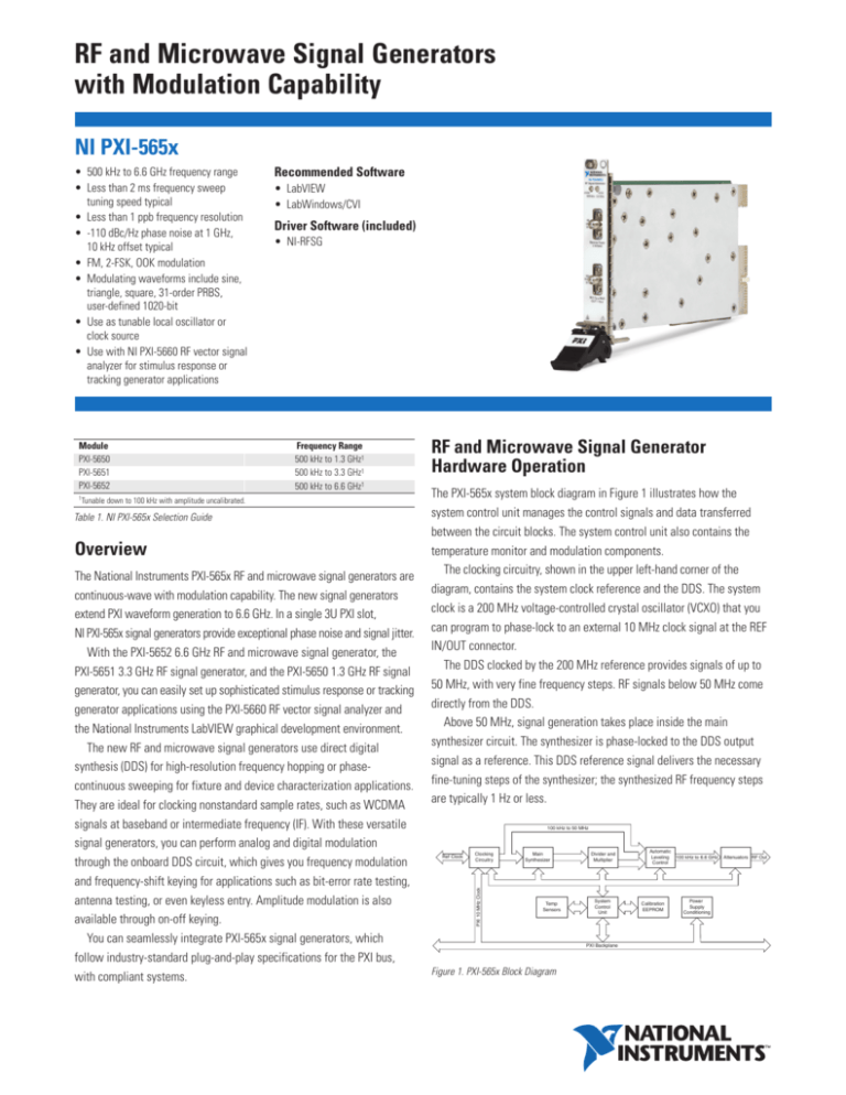
RF and Microwave Signal Generators with Modulation Capability NI PXI-565x Module PXI-5650 PXI-5651 PXI-5652 Recommended Software • LabVIEW • LabWindows/CVI Driver Software (included) • NI-RFSG Frequency Range 500 kHz to 1.3 GHz1 500 kHz to 3.3 GHz1 500 kHz to 6.6 GHz1 1 Tunable down to 100 kHz with amplitude uncalibrated. Table 1. NI PXI-565x Selection Guide Overview The National Instruments PXI-565x RF and microwave signal generators are continuous-wave with modulation capability. The new signal generators extend PXI waveform generation to 6.6 GHz. In a single 3U PXI slot, NI PXI-565x signal generators provide exceptional phase noise and signal jitter. With the PXI-5652 6.6 GHz RF and microwave signal generator, the PXI-5651 3.3 GHz RF signal generator, and the PXI-5650 1.3 GHz RF signal generator, you can easily set up sophisticated stimulus response or tracking generator applications using the PXI-5660 RF vector signal analyzer and the National Instruments LabVIEW graphical development environment. The new RF and microwave signal generators use direct digital synthesis (DDS) for high-resolution frequency hopping or phasecontinuous sweeping for fixture and device characterization applications. They are ideal for clocking nonstandard sample rates, such as WCDMA signals at baseband or intermediate frequency (IF). With these versatile signal generators, you can perform analog and digital modulation through the onboard DDS circuit, which gives you frequency modulation and frequency-shift keying for applications such as bit-error rate testing, antenna testing, or even keyless entry. Amplitude modulation is also available through on-off keying. You can seamlessly integrate PXI-565x signal generators, which follow industry-standard plug-and-play specifications for the PXI bus, with compliant systems. RF and Microwave Signal Generator Hardware Operation The PXI-565x system block diagram in Figure 1 illustrates how the system control unit manages the control signals and data transferred between the circuit blocks. The system control unit also contains the temperature monitor and modulation components. The clocking circuitry, shown in the upper left-hand corner of the diagram, contains the system clock reference and the DDS. The system clock is a 200 MHz voltage-controlled crystal oscillator (VCXO) that you can program to phase-lock to an external 10 MHz clock signal at the REF IN/OUT connector. The DDS clocked by the 200 MHz reference provides signals of up to 50 MHz, with very fine frequency steps. RF signals below 50 MHz come directly from the DDS. Above 50 MHz, signal generation takes place inside the main synthesizer circuit. The synthesizer is phase-locked to the DDS output signal as a reference. This DDS reference signal delivers the necessary fine-tuning steps of the synthesizer; the synthesized RF frequency steps are typically 1 Hz or less. 100 kHz to 50 MHz Ref Clock Clocking Circuitry PXI 10 MHz Clock • 500 kHz to 6.6 GHz frequency range • Less than 2 ms frequency sweep tuning speed typical • Less than 1 ppb frequency resolution • -110 dBc/Hz phase noise at 1 GHz, 10 kHz offset typical • FM, 2-FSK, OOK modulation • Modulating waveforms include sine, triangle, square, 31-order PRBS, user-defined 1020-bit • Use as tunable local oscillator or clock source • Use with NI PXI-5660 RF vector signal analyzer for stimulus response or tracking generator applications Main Synthesizer Temp Sensors Divider and Multiplier System Control Unit PXI Backplane Figure 1. PXI-565x Block Diagram Automatic Leveling Control Calibration EEPROM 100 kHz to 6.6 GHz Power Supply Conditioning Attenuators RF Out RF and Microwave Signal Generators with Modulation Capability Following the main synthesizer are dividers and multipliers to scale the frequency over the range of 50 MHz to the upper frequency limit of PXI-565x signal generators. The automatic leveling control (ALC) loop performs fine amplitude control. The ALC has a broad frequency response, typically from a few kilohertz to more than 6.6 GHz. A temperature-stable voltage digital-toanalog converter (DAC) sets the reference for the ALC. Additional temperature calibration performed during the manufacturing process makes the ALC very stable over the specified operating temperature. Attenuators (final block of the system) perform coarse amplitude control. These attenuators have a typical range of 100 dB. The NI-RFSG instrument driver uses calibration data stored in the EEPROM to correctly set up the hardware for signal generation. The instrument driver uses calibration data to compensate for nonideal components and temperature variation. Refer to Understanding Factory Calibration in the NI RF Signal Sources Help for more information. Modulation Modes PXI-565x RF signal generators can generate three types of modulated signals, including: • Frequency-shift keying signals • On-off keying signals • Frequency modulated signals Frequency-Shift Keying (FSK) PXI-565x signal generators are capable of producing a 2-FSK signal. You can control the following modulation parameters: • Internal modulation waveform types – 1020-bit, user-defined bit stream, or pseudorandom bit sequence (PRBS) • Symbol rate • FSK deviation NI-RFSG calculates the exact symbol rate and FSK deviation, which can differ slightly from the input parameters. On-Off Keying (OOK) OOK is a modulation scheme that varies the power level of the carrier signal between two discrete power levels. You can control the following modulation parameters: • Internal modulation waveform type – PRBS • Symbol rate A bit value of 1 sets the carrier signal power to the configured power level. A bit value of 0 sets the carrier signal power to the lowest possible level for this frequency. Refer to your device specifications document for minimum and maximum power levels. Digital Modulating Waveform Resulting OOK Modulated Output Signal Figure 2. On-Off Keying Overview Frequency Modulation (FM) You can control the following modulation parameters: • Internal modulation waveform types – square, sine, triangle • Modulation waveform frequency • FM deviation Output Enable You can disable signal output at the RF OUT connector using the Output Enabled property. In addition, you can change the output enable state at any time during waveform generation, and the generation continues on internally. Calibration PXI-565x signal generator calibration is relative to an NIST-traceable standard over the specified operating temperature range. Calibration consists of two major parts – frequency accuracy calibration and amplitude accuracy calibration. Calibration certificates are available on request. Software The NI PXI-565x is shipped with NI-RFSG, a fully functional instrument driver compatible with a variety of application software environments, such as NI LabVIEW, LabWindows/CVI, and C. Also included are a number of interactive, instructional examples and interactive online help guides that can assist you in jump-starting your application test development. For more information, consult the NI RF Signal Sources Help. Ordering Information NI PXI-5652............................................................................779670-02 NI PXI-5651............................................................................779670-01 NI PXI-5650............................................................................779670-00 Includes NI-RFSG instrument driver software. BUY NOW! For complete product specifications, pricing, and accessory information, call (800) 813 3693 (U.S.) or go to ni.com/rf. BUY ONLINE at ni.com or CALL (800) 813 3693 (U.S.) 2 RF and Microwave Signal Generators with Modulation Capability Jitter (seconds, rms) at 0 dBm Output Power Specifications 622 MHz with 1 kHz to 5 MHz jitter BW .................................. <200 fs typical See detailed specifications for more information. NI PXI-565x RF Signal Generator This document lists specifications for NI PXI-565x RF Signal Generators. Minimum or maximum specifications are warranteed under the following conditions: • 30 minutes warm-up time at ambient temperature • Calibration cycle maintained • Temperature 0 to 55 °C unless otherwise noted. Typical values are used to define an average unit measured at ambient temperatures of 15 to 35 °C. Specifications that do not list a tolerance are typical values unless otherwise specified. Tolerance values represent the maximum variation that will be observed. Frequency 2.488 GHz with 5 kHz to 15 MHz jitter BW ................................ <50 fs typical Residual FM (300 Hz to 3 kHz, CCITT, rms) Residual FM <0.8 Hz rms <1.5 Hz rms Frequency 1.0 GHz 2.4 GHz Harmonics at ≤0 dBm Output Power Frequency 500 kHz to 1.3 GHz 1.3 to 3.3 GHz 3.3 to 6.6 GHz Harmonic (Typical) -15 dBc -25 dBc -20 dBc Range PXI-5650 .............................................. 500 kHz1 to 1.3 GHz PXI-5651 .............................................. 500 kHz1 to 3.3 GHz PXI-5652 .............................................. 500 kHz1 to 6.6 GHz 1Tunable Resolution Step Size <1 Hz <2 Hz <4 Hz Settling Time 0.1 ppm of final frequency.................. <5 ms 0.01 ppm of final frequency................ <20 ms >1 kHz Offset <-65 dBc <-65 dBc <-50 dBc >100 kHz Offset <-75 dBc <-70 dBc <-65 dBc Subharmonic Products Frequency 500 kHz to 3.3 GHz 3.3 to 4 GHz 4 to 6.6 GHz 2No Reference Clock Subharmonic Products Not applicable 2 <-30 dBc <-25 dBc harmonic multiplication in this band. Amplitude Internal Clock Initial accuracy.................................... ±3 ppm max. Temperature (15 to 35 °C) ................. ±1 ppm max. Aging .................................................. ±5 ppm/year max. Spectral Purity SSB Phase Noise at 10 kHz Offset Frequency 100 MHz 500 MHz 1 GHz 3 GHz 6.6 GHz Nonharmonic Products Frequency 500 kHz to 50 MHz 50 MHz to 3.3 GHz 3.3 to 6.6 GHz down to 100 kHz with amplitude uncalibrated. Frequency 500 kHz to 1.3 GHz 1.3 to 3.3 GHz 3.3 to 6.6 GHz Nonharmonics at ≤0 dBm Output Power Phase Noise <-125 dBc/Hz <-112 dBc/Hz <-105 dBc/Hz <-95 dBc/Hz <-90 dBc/Hz Resolution ........................................... <0.1 dB Range3 ................................................. -100 to 10 dBm 3See detailed specifications for frequency specific amplitude ranges. Power Level Accuracy (15 °C to 35 °C) Less than 3.3 GHz >-40 dBm......................................... <-40 dBm......................................... Greater than 3.3GHz >-40 dBm......................................... <-40 dBm......................................... ±0.75 dB ±1.8 dB ±1.0 dB ±2.0 dB Amplitude Settling Time 0.25 dB of final value.......................... <10 ms typical 0.05 dB of final value.......................... <500 ms typical BUY ONLINE at ni.com or CALL (800) 813 3693 (U.S.) 3 RF and Microwave Signal Generators with Modulation Capability Signal to Noise Ratio Frequency Shift Keying (FSK) ≥0 dBm output power......................... <-140 dBc/Hz typical Modulation waveform types PRBS ............................................... 5 to 31-order User defined ................................... up to 1020 bit Modulation format.............................. 2-FSK VSWR 500 kHz to 3.3 GHz.............................. <1.8:1 typical 3.3 to 6.6 GHz ..................................... <2.0:1 typical Output impedance............................... 50 Ω Modulation Frequency Modulation (FM) Modulation waveform types............... Sine, triangle, square Frequency Range 500 kHz to <50 MHz ≥50 to <100 MHz ≥100 to <200 MHz ≥200 to <400 MHz ≥400 to <800 MHz ≥800 MHz to <1.6 GHz ≥1.6 to <3.3 GHz ≥3.3 to <6.6 GHz Modulation waveform frequency4 ...... Deviation accuracy5 ............................ Distortion5 ........................................... SINAD5 ................................................ 4Settable 51 Maximum Deviation (Sine Wave) 500 kHz 125 kHz 250 kHz 500 kHz 1 MHz 2 MHz 4 MHz 8 MHz 1 Hz to 100 kHz <±3.5% <0.1% >65 dB frequencies are given by 50 MHz/k, where k is an even integer up to 226 kHz sine wave, 10% of maximum deviation; noise bandwidth of 10 kHz Frequency Range 500 kHz to <50 MHz ≥50 to <100 MHz ≥100 to <200 MHz ≥200 to <400 MHz ≥400 to <800 MHz ≥800 MHz to <1.6 GHz ≥1.6 to <3.3 GHz ≥3.3 to <6.6 GHz Maximum Deviation 250 kHz 31.25 kHz 62.5 kHz 125 kHz 250 kHz 500 kHz 1 MHz 2 MHz FSK deviation accuracy (100 kHz rate, 10% of maximum deviation)............... <±10% Symbol rate......................................... 763 Hz to 100 kHz On-Off Keying (OOK) Modulation waveform types............... 5 to 31-order PRBS Power level <10 MHz.......................................... typically 7 dBm below maximum specified amplitude >10 MHz.......................................... typically 10 dBm below maximum specified amplitude Symbol rate......................................... 153 Hz to 100 kHz BUY ONLINE at ni.com or CALL (800) 813 3693 (U.S.) 4
