5 - UCLA Physics & Astronomy
advertisement
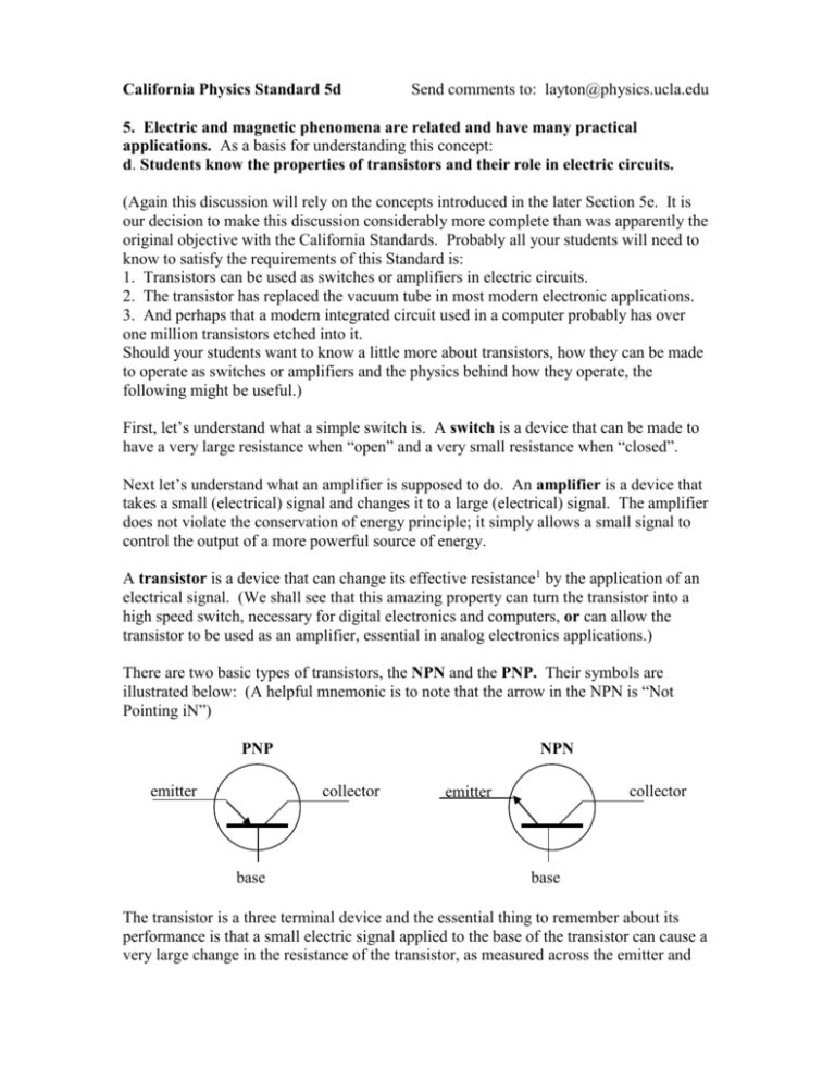
California Physics Standard 5d Send comments to: layton@physics.ucla.edu 5. Electric and magnetic phenomena are related and have many practical applications. As a basis for understanding this concept: d. Students know the properties of transistors and their role in electric circuits. (Again this discussion will rely on the concepts introduced in the later Section 5e. It is our decision to make this discussion considerably more complete than was apparently the original objective with the California Standards. Probably all your students will need to know to satisfy the requirements of this Standard is: 1. Transistors can be used as switches or amplifiers in electric circuits. 2. The transistor has replaced the vacuum tube in most modern electronic applications. 3. And perhaps that a modern integrated circuit used in a computer probably has over one million transistors etched into it. Should your students want to know a little more about transistors, how they can be made to operate as switches or amplifiers and the physics behind how they operate, the following might be useful.) First, let’s understand what a simple switch is. A switch is a device that can be made to have a very large resistance when “open” and a very small resistance when “closed”. Next let’s understand what an amplifier is supposed to do. An amplifier is a device that takes a small (electrical) signal and changes it to a large (electrical) signal. The amplifier does not violate the conservation of energy principle; it simply allows a small signal to control the output of a more powerful source of energy. A transistor is a device that can change its effective resistance1 by the application of an electrical signal. (We shall see that this amazing property can turn the transistor into a high speed switch, necessary for digital electronics and computers, or can allow the transistor to be used as an amplifier, essential in analog electronics applications.) There are two basic types of transistors, the NPN and the PNP. Their symbols are illustrated below: (A helpful mnemonic is to note that the arrow in the NPN is “Not Pointing iN”) PNP emitter NPN collector base collector emitter base The transistor is a three terminal device and the essential thing to remember about its performance is that a small electric signal applied to the base of the transistor can cause a very large change in the resistance of the transistor, as measured across the emitter and the collector. To understand how this might be useful, let’s look again at the simple electric circuit involving a battery and two resistors in series: V battery When a transistor replaces the lower resistor, a small change in the input voltage can cause a large change in the output voltage. If the battery voltage remains constant and the resistance of the lower resistor could somehow be made to get larger V output and smaller, the “output” voltage across the lower resistor will also get larger and smaller. V in There are details that must be added to this circuit before it can be used as an amplifier or a switch, but the important idea to appreciate is that a small signal on the input to the transistor’s base can make a large change in its resistance and therefore make a large change in the output voltage across the transistor. We will discuss the physics behind what makes a transistor display this property later, but for now, the essential idea to understand is that a small change in the electrical signal at the base of a transistor can cause a very large change in the resistance of the transistor, as measured across the emitter and collector. How transistors, diodes and other solid state electronic devices do what they do. Elements in the center of the periodic chart such as carbon, germanium and silicon, are usually semiconductors. Since carbon has an extremely high melting point, it is essentially impossible to purify as is required in modern semiconductor devices. Germanium was the first substance used in the manufacturing of semiconductor devices but its low melting point caused these devices to be easily damaged when soldering them into circuits. When silicon, with its higher melting point, was developed for use in semiconductor devices, it rapidly became the universal material for most electronic applications. Most diodes, transistors and integrated circuits in use today use silicon as the primary semiconductor material. Pure Silicon is an insulator. The Silicon atom has 4 outer valence electrons. If pure silicon is “doped” with a small amount of material with 5 valence electrons, the result is an N type semiconductor that conducts by electron, or negative charge flow. If the silicon is “doped” with a material with 3 valence electrons, the material conducts by “holes” and replicates positive charge flow. This is called a P type semiconductor. Diodes When a P type and an N type semiconductor are joined together, a solid-state diode is formed. When the P is attached to the plus side of a source of voltage and the N is V out attached to negative side, the holes and electrons are driven together at the junction and any voltage above a minimum amount (0.7 volts for silicon) will cause the diode to conduct. If the polarity is reversed, the holes and electrons are pulled apart at the junction, the diode becomes an insulator and will not conduct unless a high “breakdown potential” is exceeded. The symbol for a diode is shown below: The arrow points in the direction of conventional current when the diode is conducting. This means, if the left end is connected to plus and the right is connected to minus, conventional current will flow in the direction of the arrow. Many simple circuits have been developed using diodes that will convert AC to DC. Transistors The transistor is a three terminal device. A junction NPN transistor consists of a thin piece of P type semiconductor sandwiched between two pieces of N type semiconductor. Likewise, a PNP transistor consists of a thin piece of N type semiconductor sandwiched between two pieces of P type semiconductor. The internal makeup and corresponding symbol of each type of transistor is shown below: On the left is a PNP transistor and on the right is a NPN transistor. (To help you remember, NPN could stand for “not pointing in”.) The electrode with the arrow is called the emitter*, the flat electrode in the center is called the base and the one to the left with no arrow is called the collector. A quick explanation of how the transistor works follows: The power source is connected across emitter and collector with the collector reverse biased. (For example, the collector in an NPN transistor would be connected to the positive pole of the battery and the emitter to the negative pole.) The transistor will not conduct since the base collector diode is reverse biased. However, the holes in the P type base are driven toward the N type emitter and if the plus signal voltage is higher than 0.7 volts (for silicon) the holes will cross the junction, combine with the electrons in the emitter and give them enough energy to cross into the base. Since the base is very thin, the electrons can be given enough energy to cross into the collector and cause a *The arrow on the emitter symbol indicates conventional current. A very small signal voltage can cause a current direction when the transistor is conducting. current into the much higher voltage power circuit, amplifying the signal. 1. Use of the term “effective resistance” will be replaced with simply the word “resistance” in further discussions. Since we have introduced the definition of resistance earlier in this section and since the more general term “impedance” will not be a part of the Standards, we choose to use the more familiar term resistance, even if it is not strictly accurate in this context.

