Spin polarized transport in semiconductors – Challenges for

Contribution (Oral/Poster/Keynote)
Nanoscopic investigation of advanced dielectrics for innovative electric devices
Raffaella Lo Nigro , Patrick Fiorenza and Vito Raineri
Consiglio Nazionale delle Ricerche - Istituto per la Microelettronica e Microsistemi (CNR-IMM) Strada
VIII n. 5, Zona Industriale, 95121 Catania – Italy e-mail:raffaella.lonigro@imm.cnr.it
Everyday we are surrounded by electronic devices which overheat, transmit great amount of electromagnetic waves and whose weight and size sometimes seem not so comfortable. Therefore, it appears greatly desirable the availability of integrated devices of high efficiency with reduced power consumption and/or low intensity transmission of electromagnetic radiation, furthermore overcoming current hot topics in nowadays society, such as energy saving, environmental protection and human health. For all these reasons the European initiative on “Nanoscience, advanced materials and innovative processing (NMP)” prompt and sustain the development of advanced research based on fundamental physical-chemical properties of new dielectric materials.
Every new material strongly needs of both microscopic and nanoscopic investigation, in fact a deep understand of the dielectric properties such as conduction mechanisms and/or reliability takes advantages from nanoscopic techniques to better control defects and impurities.
Here we propose our research focused on the development of specific methodologies and new methods based on microscopy scanning probe for characterization at the nanoscale, which is very important to control the materials characteristics and performances.
The investigated materials have been thin solid films of praseodymium oxides high k dielectrics [1,2] as alternative to SiO
2
in C-MOS devices and of calcium copper titanate (CaCu
3
Ti
4
O
12
) giant k materials [3-
5] as alternative to ferroelectrics in low-emission antennas and condensers. Both materials have been studied by Scanning Capacitance Microscopy (SCM) and Conductive –Atomic Force Microscopy (C-
AFM).
In regards to the praseodymium based dielectrics, several oxides ( high-k Pr
2
O
3
and PrAlO
3
)[1,6], both simple and complex, have been investigated producing a quite established basic knowledge. The principal aspects which have been evaluated are:
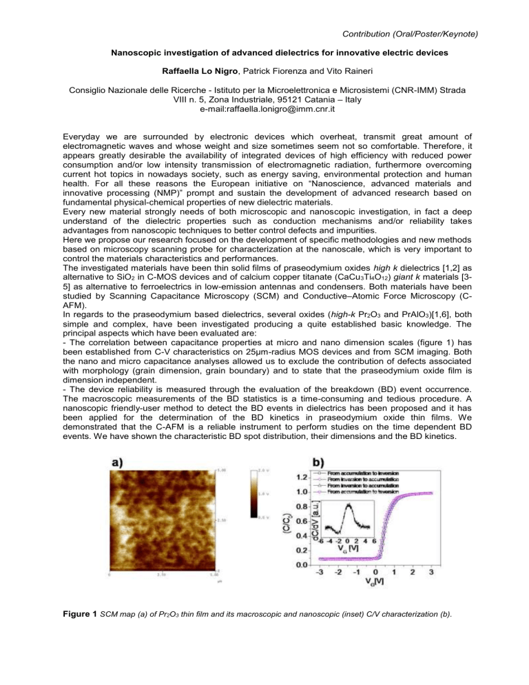
- The correlation between capacitance properties at micro and nano dimension scales (figure 1) has been established from CV characteristics on 25μm-radius MOS devices and from SCM imaging. Both the nano and micro capacitance analyses allowed us to exclude the contribution of defects associated with morphology (grain dimension, grain boundary) and to state that the praseodymium oxide film is dimension independent.
- The device reliability is measured through the evaluation of the breakdown (BD) event occurrence.
The macroscopic measurements of the BD statistics is a time-consuming and tedious procedure. A nanoscopic friendly-user method to detect the BD events in dielectrics has been proposed and it has been applied for the determination of the BD kinetics in praseodymium oxide thin films. We demonstrated that the C-AFM is a reliable instrument to perform studies on the time dependent BD events. We have shown the characteristic BD spot distribution, their dimensions and the BD kinetics.
Figure 1 SCM map (a) of Pr
2
O
3
thin film and its macroscopic and nanoscopic (inset) C/V characterization (b).
Contribution (Oral/Poster/Keynote)
In regards to the CaCu
3
Ti
4
O
12, one of the more discussed aspect, in the literature [7-9], is related to the mysterious origin of its giant dielectric properties. The discussion is centred on the possibility of explaining the origin as an intrinsic property or due to extrinsic mechanisms. Recent studies tend to support the extrinsic mechanism, whereby the grain boundaries consist of semiconductor/insulator defects due to oxygen ions and/or planar defects that make the very large dielectric constant through a mecha nism known as "internal barrier layer capacitors” [7,8]. Thus, the macroscopic properties of dielectrics often depend on the local behavior of physical phenomena at the nanoscale. Examples are the transport properties of the grain boundaries, the different electrical properties of nanoprecipitates and of any other phases.
Here, the nanoscale imaging of electrical properties in materials with giant permittivity have been performed. Scanning capacitance microscopy and C-AFM (figure 2) is proposed to investigate the mechanisms involved in the giant permittivity phenomena in terms of electrical inhomogeneity detection
[10]. We report on the characterization of CaCu
3
Ti
4
O
12
materials confirming the presence of the grain boundary effect, to date only hypnotized on the basis of microscopic measurements, and discovering electrical domains within the single grain.
Morphology
C-AFM
50nm
0
100pA
0
-100pA
20 μm
Figure 2 Morphologic characterization and C-AFM map (a) of CCTO materials.
Generally, the scanning capacitance microscopy has been used as innovative tool for the determination the local dielectric properties, while conductive atomic force microscopy has been employed to measure the local transport current within grains and at the grain boundaries.
In a larger perspective, the present research activity is focused on the study of new dielectric materials aiming to understand their intrinsic and extrinsic properties and looking for some routes to tailor the dielectric properties. Moreover, as a further and ambitious challenge, new dielectrics for next generation electronics are considered for the realization of new integrated circuits as a possible alternative to silicon technology.
References
[1] R. Lo Nigro, R. Toro, G. Malandrino, V. Raineri, I. L. Fragalà, Adv. Mater. 15 (2003) 1071.
[2] R. Lo Nigro, R. G. Toro, G. Malandrino, G. G. Condorelli, V. Raineri, I. L. Fragalà, Adv. Funct. Mater.
15 (2005) 838.
[3]R. Lo Nigro, R. Toro, G. Malandrino, M. Bettinelli, A. Speghini, I. L. Fragalà, Adv. Mater. 16 (2004)
891.
[4] R. Lo Nigro, G. M alandrino, R.G. Toro, M. Losurdo, G. Bruno, I. L. Fragalà, J. Am. Chem. Soc. 127
(2005) 13772.
[5] R. Lo. Nigro, R.G. Toro, G. Malandrino, I. L. Fragalà, M. Losurdo, M. M. Giangregorio, G. Bruno, V.
Raineri, P. Fiorenza, J. Phys. Chem. B 110 (2006) 17460.
[6] R. Lo Nigro, R.G. Toro , G. Malandrino, I. L. Fragalà. Chem. Mater. 19 (2007) 4442.
[7] T. B. Adams, D. C. Sinclair, A. R West, Adv. Mater. 14 (2002) 1321
[8] D. C. Sinclair, T. B. Adams, F. D. Morrison, A. R West, Appl. Phys. Lett. 80 (2002) 2153.
[9] C. C.Homes, T.Vogt, S. M. Shapiro,S. Wakimoto, A. P. Ramirez , Science 293 (2001) 217.
[10] P. Fiorenza, R. Lo Nigro, S. Sciuto, P. Delugas, V. Raineri, R. G. Toro, M. R. Catalano, G.
Malandrino, J. Appl. Phys. 109 (2009) 061634.


