Reducing Switching Capacitance Using Buffers
advertisement

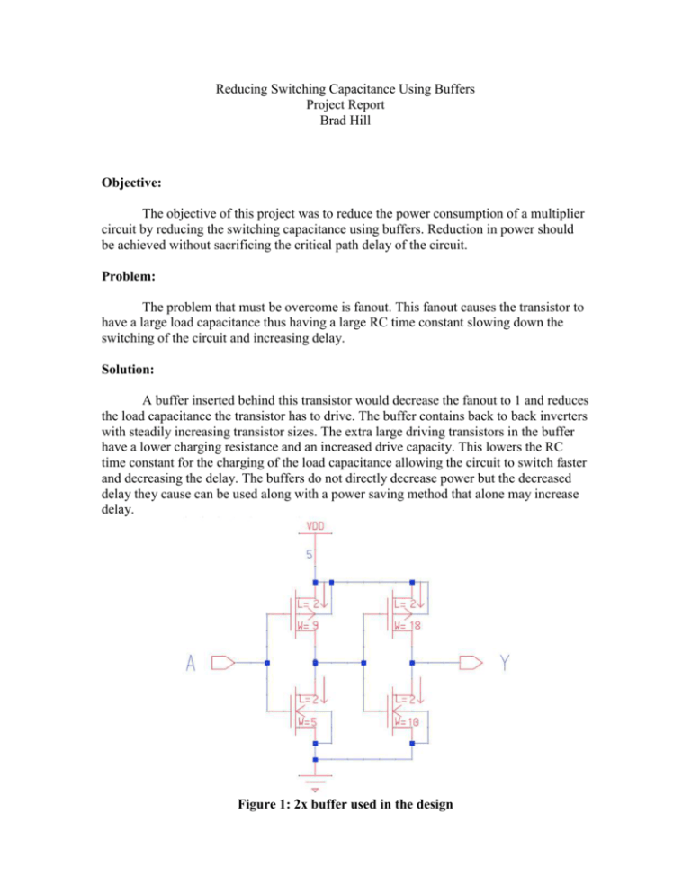
Reducing Switching Capacitance Using Buffers Project Report Brad Hill Objective: The objective of this project was to reduce the power consumption of a multiplier circuit by reducing the switching capacitance using buffers. Reduction in power should be achieved without sacrificing the critical path delay of the circuit. Problem: The problem that must be overcome is fanout. This fanout causes the transistor to have a large load capacitance thus having a large RC time constant slowing down the switching of the circuit and increasing delay. Solution: A buffer inserted behind this transistor would decrease the fanout to 1 and reduces the load capacitance the transistor has to drive. The buffer contains back to back inverters with steadily increasing transistor sizes. The extra large driving transistors in the buffer have a lower charging resistance and an increased drive capacity. This lowers the RC time constant for the charging of the load capacitance allowing the circuit to switch faster and decreasing the delay. The buffers do not directly decrease power but the decreased delay they cause can be used along with a power saving method that alone may increase delay. Figure 1: 2x buffer used in the design Multiplier: A 32x32 bit multiplier was created and simulated to verify its correctness. However, to start trying to reduce the power on such a large circuit would be too advantageous. Power reduction started with just one cell, inserting buffers in the proper places to reduce the delay in the circuit. The best placement of buffers to reduce delay turned out to be on the Carry_in and Sum_in inputs into the multiplier cell. Figure 2: Cell with buffers These input lines had the largest fanout, both with 6 transistors to drive. Simulation with all the possible vectors was used to determine the power consumption of a cell both with and without buffers. A 90% of full value of the input to 90% of full value of the slowest output was used to determine delay. However, using the 50% marks would have yielded a more accurate estimate of delay. Below are the screen captures of the delay plots. The VDD used is 1.8V. Figure 3: Delay Plot of Cell with no Buffers Figure 4: Delay Plot of Cell with Buffers The comparison chart will show a large decrease in the delay of the cell with the buffers in place this allows a decrease in the supply voltage to decrease the power. Alone reducing the supply voltage would decrease the power but would push the delay over the critical delay which in this project is unacceptable. The supply voltage was reduced to 1.75V. Even though there is just a slight decrease in voltage the decrease in power and increase in delay are noticeable. Figure 5: Delay of Cell at 1.75V and no Buffers As seen in the plot the delay of the circuit went up as expected with the decrease of supply voltage. Figure 6: Delay of Cell with Buffers at 1.75V As seen in this plot the delay did increase from before but is still well below the delay of the cell at 1.8V and no buffers. The comparison table shows in detail the results from the simulation. Dynamic(W) Static(W) Delay(S) Supply Voltage Single Cell 33.86u 171.14p 14.942p 1.8V Cell with buffers 35.08u 243.98p -129.56p 1.8V No Buffers 31.44u 162.10p 16.129p 1.75V Buffers 32.34u 230.87p -120.778p 1.75V Difference -1.52u 59.73p -135.72p -0.05V Figure 7: Comparison Table of Results The lines in green show the results of the simulation of the cell with no buffers at 1.8V and a cell with buffers at 1.75V. The power has been reduced while the delay is still at an acceptable level. An elimination of the glitch in the output is another benefit from the buffers. A multi-cell configuration was also simulated. The best placement of buffers in this configuration is a buffer on all the inputs of the first cell and no buffers in the second cell. Figure 8: Two Cells with Buffers The power and delay of two cells were simulated using all possible vectors. The comparison table shows a drastic decrease in power with still a substantial decrease in delay with just a 0.05V reduction in supply voltage. Dynamic(W) Static(W) Delay(S) Supply Voltage No Buffers 467.126u 342.282p 12.081p 1.8V Buffers 488.136u 487.96p -7.85p 1.8V No Buffers 418.677u 324.2060p 13.510p 1.75V Buffers 438.90u 461.75p 5.095p 1.75V Difference -28.226u 119.552p -6.986p -0.05V Figure 9: Two Cell Comparison Table A 28.226uW savings in power was achieved with just this little drop in supply voltage. Refer to the presentation to see the plot of the delay. The area increase the buffers cause is only 17.36%. Conclusion: Strategically placed buffers in a circuit can greatly reduce the delay of this circuit. This reduction in delay can be used along side a method of reducing power that on its own would increase the delay to an undesirable level. A circuit with a higher fanout would benefit even more from buffers.


