ch05
advertisement
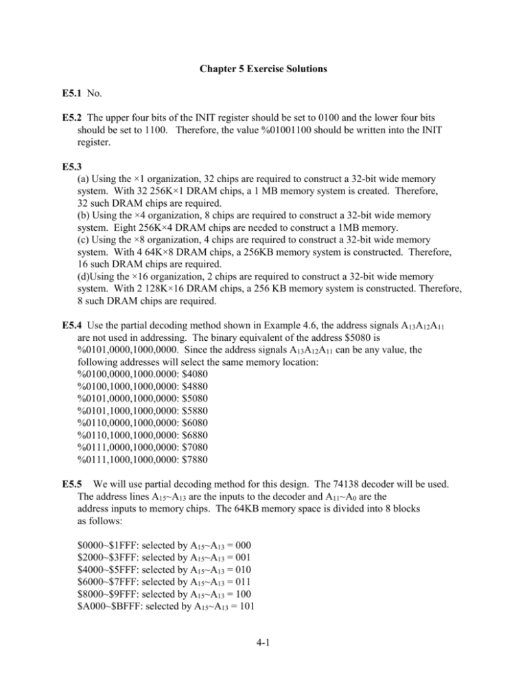
Chapter 5 Exercise Solutions E5.1 No. E5.2 The upper four bits of the INIT register should be set to 0100 and the lower four bits should be set to 1100. Therefore, the value %01001100 should be written into the INIT register. E5.3 (a) Using the ×1 organization, 32 chips are required to construct a 32-bit wide memory system. With 32 256K×1 DRAM chips, a 1 MB memory system is created. Therefore, 32 such DRAM chips are required. (b) Using the ×4 organization, 8 chips are required to construct a 32-bit wide memory system. Eight 256K×4 DRAM chips are needed to construct a 1MB memory. (c) Using the ×8 organization, 4 chips are required to construct a 32-bit wide memory system. With 4 64K×8 DRAM chips, a 256KB memory system is constructed. Therefore, 16 such DRAM chips are required. (d)Using the ×16 organization, 2 chips are required to construct a 32-bit wide memory system. With 2 128K×16 DRAM chips, a 256 KB memory system is constructed. Therefore, 8 such DRAM chips are required. E5.4 Use the partial decoding method shown in Example 4.6, the address signals A13A12A11 are not used in addressing. The binary equivalent of the address $5080 is %0101,0000,1000,0000. Since the address signals A13A12A11 can be any value, the following addresses will select the same memory location: %0100,0000,1000.0000: $4080 %0100,1000,1000,0000: $4880 %0101,0000,1000,0000: $5080 %0101,1000,1000,0000: $5880 %0110,0000,1000,0000: $6080 %0110,1000,1000,0000: $6880 %0111,0000,1000,0000: $7080 %0111,1000,1000,0000: $7880 E5.5 We will use partial decoding method for this design. The 74138 decoder will be used. The address lines A15~A13 are the inputs to the decoder and A11~A0 are the address inputs to memory chips. The 64KB memory space is divided into 8 blocks as follows: $0000~$1FFF: selected by A15~A13 = 000 $2000~$3FFF: selected by A15~A13 = 001 $4000~$5FFF: selected by A15~A13 = 010 $6000~$7FFF: selected by A15~A13 = 011 $8000~$9FFF: selected by A15~A13 = 100 $A000~$BFFF: selected by A15~A13 = 101 4-1 $C000~$DFFF: selected by A15~A13 = 110 $E000~$FFFF: selected by A15~A13 = 111 Since the reset vector is in ROM1, we must assign the block $E000~$FFFF to ROM1. We will assign the space $6000~$7FFF to SRAM1 and the space $8000~$9FFF to ROM2. The decoder will look as follows: 74138 A15 A14 A13 E E3 E1 E2 O0 O1 O2 O3 O4 O5 O6 O7 SRAM1 ROM2 ROM1 Figure S4.1 Decoder circuit design E5.6 We will assume that there are some other devices to be interfaced to the 68HC11. We will also assume that the reset and interrupt vectors are located in this memory chip. Therefore, we will assign the address space $E000~$FFFF to the EPROM. The circuit connection is shown in Figure S4.2. The 74F138 has a delay of 8 ns and the 74F373 latch has a delay of 11.5 ns at room temperature. Since A15~A13 are asserted 94 ns before the rising edge of the E clock and the decoder is enabled by the E clock, the decoder output will be asserted after the rising edge of the E clock. The CE input to the EPROM is asserted 8 ns after the rising edge of the E clock signal. Three groups of signals, A12~A0, CE, and OE, together decide the actual access time of the Am27C64 EPROM. Since OE signal is asserted permanently, it is irrelevant in determining the access time. The CE signal is asserted the latest, therefore, the data from the EPROM will be available 128 ns after the rising edge of the E clock or 94 ns (222 - 128) before the rising edge of the E clock. This easily satisfied the data set up requirement from the 68HC11 (30 ns at 2 MHz). The data output from the Am27C64 becomes invalid as soon as one of the three groups of signals becomes invalid. The address inputs to the EPROM remain stable for 33 ns after the falling edge of the E clock and the CE signal becomes invalid 8 ns after the falling edge of the E clock. Therefore, data output from the EPROM will remain stable only for 8 ns and hence cannot satisfy the requirement of the 68HC11. Since the 68HC11 does not drive the multiplexed address/data bus for 128 ns after the falling edge of the E clock, the capacitance of the data bus may hold the data from the memory for a short time period and satisfies the data hold time requirement. 4-2 68HC11 A15 A14 A13 E 74F138 A2 O7 A1 A0 E3 E2 E1 CE Am27C64 A12~ A8 AS AD7~ AD0 A12~ A0 74F373 LE O7~ O0 D7~D0 OE OE DQ7~ DQ0 Figure S4.2 Circuit that interface Am29C64 to 68HC11 E5.7 The decoder outputs can be asserted only if the address input A12 is high. Therefore, the decoder outputs select the following address ranges: O0: $1000 ~ $1FFF O1: $3000 ~ $3FFF O2: $5000 ~ $5FFF O3: $7000 ~ $7FFF O4: $9000 ~ $9FFF O5: $B000 ~ $BFFF O6: $D000 ~ $DFFF O7: $F000 ~ $FFFF E5.8 (a) A15~A8 are unknown for 100 ns (=227 - 33 - 94) which is the period corresponding to the hatched area in Figure 4.11. A15~A8 are in high impedance state for 0 ns. (b) There are three intervals during which A7/D7~A0/D0 are unknown. The first interval occurs when the E clock signal is low. This interval lasts for 110 ns (227 - 33 - 84). The second interval during which signals A7/D7~A0/D0 are unknown occurs around the rising edge of the E clock and its duration cannot be computed. The third interval during which A7/D7~A0/D0 are unknown occurs when the E clock is high and its duration cannot be computed because the timing diagram of the 68HC11 read bus cycle does not provide that information. The duration during which A7/D7~A0/D0 are in high impedance state cannot be computed because there is an unspecified interval during which these signals are unknown. 4-3
