LAYOUT OF A CMOS LOGIC CIRCUIT
advertisement
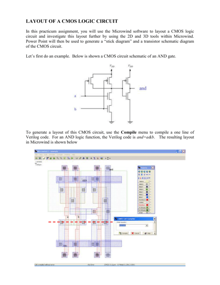
LAYOUT OF A CMOS LOGIC CIRCUIT In this practicum assignment, you will use the Microwind software to layout a CMOS logic circuit and investigate this layout further by using the 2D and 3D tools within Microwind. Power Point will then be used to generate a “stick diagram” and a transistor schematic diagram of the CMOS circuit. Let’s first do an example. Below is shown a CMOS circuit schematic of an AND gate. To generate a layout of this CMOS circuit, use the Compile menu to compile a one line of Verilog code. For an AND logic function, the Verilog code is and=a&b. The resulting layout in Microwind is shown below By using the 2D and 3D tools in the Simulate menu, one can investigate the circuit layout in greater detail. For example, use the Process Section in 2D tool to draw the dashed red line shown in the CMOS layout on the bottom of page 1. The 2D cross-section result is shown below where the cross-section of the NMOS transistors and the two layers of the metal interconnects are illustrated. Also in the Simulate menu, the Process Steps in 3D tool can be used to illustrate how the device is fabricated and can also be used to visualize the circuit in 3D. After “stepping” through the fabrication steps to build the device (up to process step #22, Metal 2 Deposition), all of these layers are illustrated below. By positioning the circuit using the “arrow tools,” the front edge of the following illustration depicts the NMOS transistors in the circuit. Compare this 3D view of the NMOS transistors with the previous 2D cross-section view of the NMOS transistors shown above. Once one has a visualization of how a CMOS circuit is laid-out, one should be able to draw a simplified layout or a “stick diagram” of this CMOS AND gate. One such diagram is shown below in a Power Point drawing. Finally, if one is to compare directly the CMOS layout with a transistor symbol diagram of the circuit (such as the first figure at the top of page 1), this can be accomplished by removing all of the layers in the layout except for the metal interconnects and then super-imposing an illustration of the transistor symbols onto this metal interconnect layout. This is illustrated below with the transistor circuit symbols and the layout of the metal interconnects. Through the use of the Microwind and Power Point software and by following the procedure presented in this document, one should be able to gain a fundamental understanding and an appreciation of how static CMOS logic functions are implemented in silicon. Lab Procedure For those seated at an odd numbered station, layout the logic function out d a b c (in Verilog code write it as out=~(d|(a&(b|c))) ), and for those seated at an even numbered station, layout the logic function f a b c d (in Verilog code write it as f=~((a|b)&(c|d)) ). Document the following in your lab notebook: 1. 2. 3. 4. 5. 6. A CMOS transistor circuit diagram of the logic function. A Microwind layout of the logic function. 2D cross-sectional views of the NMOS and PMOS transistors. 3D views of the entire CMOS circuit. A simplified layout or a “stick diagram” of the logic function in Power Point. A circuit diagram in Power Point of transistor symbols super-imposed on top of a layout of the metal interconnects so as to verify the transistor circuit diagram of the logic function.
