Details
advertisement
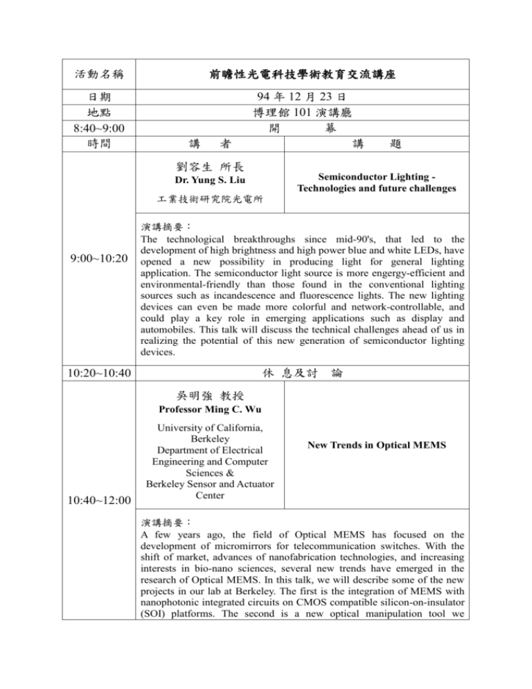
活動名稱 日期 地點 8:40~9:00 時間 前瞻性光電科技學術教育交流講座 講 者 94 年 12 月 23 日 博理館 101 演講廳 開 幕 講 題 劉容生 所長 Semiconductor Lighting Technologies and future challenges Dr. Yung S. Liu 工業技術研究院光電所 9:00~10:20 演講摘要: The technological breakthroughs since mid-90's, that led to the development of high brightness and high power blue and white LEDs, have opened a new possibility in producing light for general lighting application. The semiconductor light source is more engergy-efficient and environmental-friendly than those found in the conventional lighting sources such as incandescence and fluorescence lights. The new lighting devices can even be made more colorful and network-controllable, and could play a key role in emerging applications such as display and automobiles. This talk will discuss the technical challenges ahead of us in realizing the potential of this new generation of semiconductor lighting devices. 休 息及討 論 10:20~10:40 吳明強 教授 Professor Ming C. Wu 10:40~12:00 University of California, Berkeley Department of Electrical Engineering and Computer Sciences & Berkeley Sensor and Actuator Center New Trends in Optical MEMS 演講摘要: A few years ago, the field of Optical MEMS has focused on the development of micromirrors for telecommunication switches. With the shift of market, advances of nanofabrication technologies, and increasing interests in bio-nano sciences, several new trends have emerged in the research of Optical MEMS. In this talk, we will describe some of the new projects in our lab at Berkeley. The first is the integration of MEMS with nanophotonic integrated circuits on CMOS compatible silicon-on-insulator (SOI) platforms. The second is a new optical manipulation tool we developed at Berkeley, called optoelectronic tweezers (OET). Using photoconductor to convert optical images to reconfigurable electrodes for electrokinetic forces such as dielectrophoresis (DEP), a large number of optical traps (up to 31,000 demonstrated) can be addressed simultaneously and individually. 午 餐及休 息 12:00~13:30 陳永睿 教授 Professor Yung Jui Chen Department of Computer Science and Electrical Engineering University of Maryland, Baltimore County Future Directions of Planar Lightwave Circuits 演講摘要: 13:30~14:50 With the burst of optical communication bubble, it is clear that future direction of photonics is not limited to optical communications anymore. In my opinion, there are three major areas: optical communications/networking, optical interconnects, and optical sensors. All these applications demand more functionality and intelligence, which calls for large scale integrated optics/optoelectronics technology. Planar Lightwave circuit position itself as a key enabling technology for the future. Two of the key elements for large scale integration of planar lightwave circuits (PLC) are high index contrast waveguide material and proper device platform. In this talk I will visit the challenges and discuss these subjects in detail. I will also address the needs of a next generation OEIC technology -integration of electronic circuits and PLCs. 休 息及討 論 14:50~15:05 吳詩聰 Professor Shin-Tson Wu College of Optics and Photonics University of Central Florida 15:05~16:25 演講摘要: In this talk, I will review the recent progress in tunable liquid crystal photonic devices. A special emphasis is in tunable-focus lenses and microlens arrays. Various approaches, such as gradient refractive index nanoscale polymer-dispersed liquid crystal, polymer separated composite film, and liquid lens with changing aperture will be discussed. 休 息及討 論 16:25~16:40 16:40~18:00 Tunable Photonic Liquid Crystal Devices 鄭克勇 教授 Hyper-Uniform Nanophotonic Technologies for Ultra-Fast Optoelectronic Professor Keh-Yung Cheng Department of Electrical and Computer Engineering University of Illinois at Urbana-Champaign 演講摘要: The demonstration of ultra-fast optoelectronic interconnect systems with a speed of >100Gb/s requires the ability to design, fabricate, and integrate ultra-high-speed light sources with detectors and driver circuits. The operation speed of the optoelectronic components needs to be much faster than the system requirement. However, in conventional diode lasers used for optical communications, the time required in completing the injection and recombination process limits the maximum direct modulation speed to below 30GHz. The speed of injection and recombination processes is a function only of the materials used, and imposes a fundamental physical limit on modulation speeds of conventional laser diodes. As a result, advances in high-speed laser performance have slowed to a crawl in the last decade as today’s device structures bump up against that limit. In this talk, the program details of the Center of Hyper-Uniform Nano-photonic Technologies for Ultra-Fast Optoelectronic Systems (HUNT Center) supported by a DARPA University Photonics Research Centers program will be discussed. The program goal of the HUNT Center is to accomplish ultra-high (>50GHz) optoelectronic interconnect systems using a revolutionary ultra-fast light-emitting transistor (LET) design which could be directly modulated at a speed near THz. To realize the ultra-fast LET laser, hyper-uniform nanophotonic technologies will be developed and implemented into the laser structures. The research program of the Center encompasses the design, simulation, characterization, growth, fabrication, integration, and testing of hyper-uniform quantum dot arrays, ultra-fast light-emitting devices, near-IR optoelectronic devices, and ultra-high speed optoelectronic interconnect systems. To achieve the Center goals, the research work are divided into three cross-linked and integrated tasks including 1) hyper-uniform nanophotonic technologies development, 2) high-quality nanophotonic devices development, and 3) ultra-fast (>100GHz) light source development. Recent breakthroughs and new developments will be highlighted.
