Thermal Oxidation
advertisement
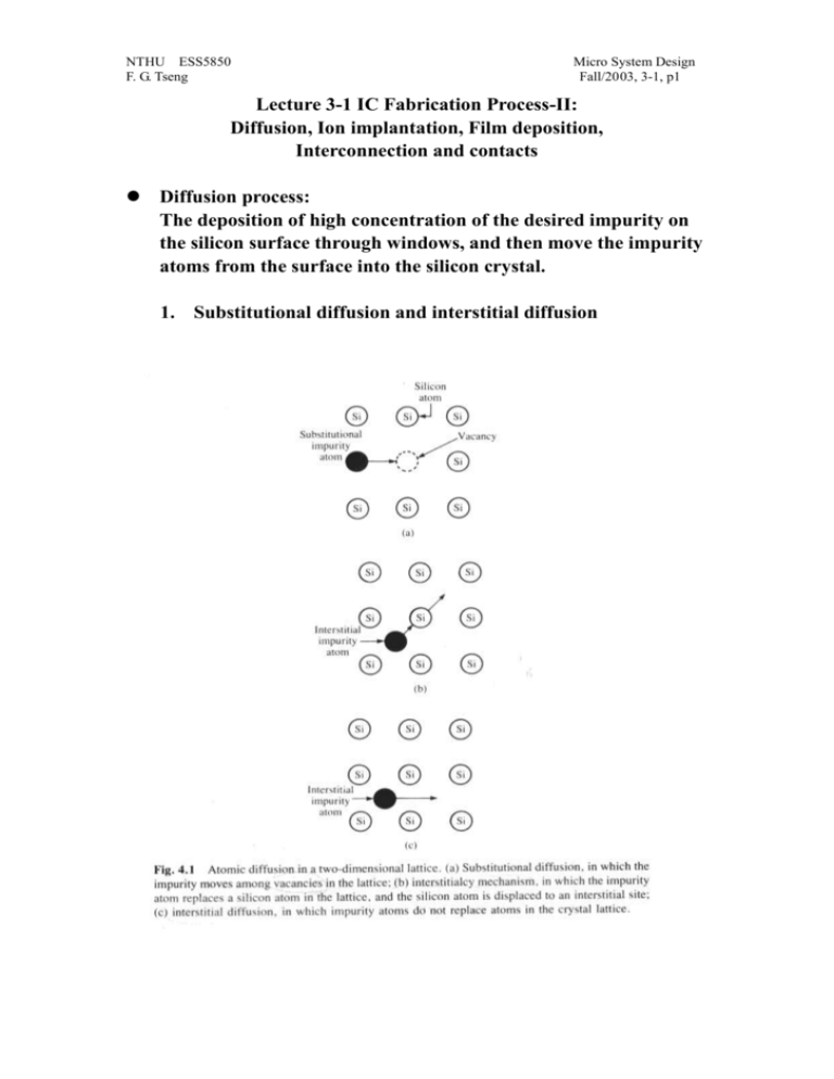
NTHU ESS5850 F. G. Tseng Micro System Design Fall/2003, 3-1, p1 Lecture 3-1 IC Fabrication Process-II: Diffusion, Ion implantation, Film deposition, Interconnection and contacts Diffusion process: The deposition of high concentration of the desired impurity on the silicon surface through windows, and then move the impurity atoms from the surface into the silicon crystal. 1. Substitutional diffusion and interstitial diffusion NTHU ESS5850 F. G. Tseng Micro System Design Fall/2003, 3-1, p2 2. Mathematical Model for diffusion: Fick’s first law of diffusion: J D N x (3-1) J: Particle flux of the donor or acceptor impurity species, N: concentration of the impurity, D: Diffusion coefficient. Continuity equation: N J t x (3-2) Combine (3-1) and (3-2) yields Fick’s second law of diffusion: N 2 N D 2 t x (3-3) Assumption: D is independent of position. 2.1Constant source diffusion: N ( x, t ) N 0 erfc( x ) 2 Dt (3-4) N0: the impurity concentration at the wafer surface The dose Q (atoms/cm2): Q N ( x, t )dx 2 N 0 Dt / 0 (3-5) NTHU ESS5850 F. G. Tseng Micro System Design Fall/2003, 3-1, p3 2.2Limited source diffusion: N ( x, t ) (Q / Dt ) exp Gaussian distribution ( x / 2 Dt ) 2 (3-6) NTHU ESS5850 F. G. Tseng Micro System Design Fall/2003, 3-1, p4 2.3Two-step diffusion: A short constant-source diffusion is often followed by a limited-source diffusion. The constant-source diffusion step is used to, establish a known dose in a shallow layer (predeposition step), then the second limited diffusion step (drive-in step) move the diffusion front to the desire depth. If Dt product of the predeposition step much greater: erfc function distribution If Dt product of the drive-in step much greater: Gaussian function distribution 2.4 Successive diffusion: ( Dt) tot Di t i i 3. Junction-Depth Measurement: (3-7) NTHU ESS5850 F. G. Tseng Micro System Design Fall/2003, 3-1, p5 4. Sheet Resistance L L R ( )( ) R s ( ) t W W (3-8) R: resistance, ρ:resistivity, L: length, W: width, t: thickness, Rs: sheet resistance. NTHU ESS5850 F. G. Tseng Micro System Design Fall/2003, 3-1, p6 5. The Four–Point Probe: 2sV / I ohm-meters for t >> s (t / ln 2)V / I ohm-meters for s >> t NTHU ESS5850 F. G. Tseng Micro System Design Fall/2003, 3-1, p7 6. Diffusion System: 6.1 Boron diffusion: · Surface concentration can be: 4×10²⁰/cm3 · Use boron trioxide (B2O3) to introduce boron—hard to strip=>use short oxidation step to help strip · 2 B2 O3 3Si 4B 3SiO2 · Solid source: Trimethylborate (TMB), or Boron Nitride C 2(CH 3 O) 3 B 9O2 900 B2 O3 6CO2 9 H 2 O · Liquid source: boron tribromide (BBr3) 4BBr3 3O2 2 B2 O3 6 Br2 · Gaseous source: diborane (B2H6), poisonous and explosive, diluted with 99.9% Ar or N2 C B2 H 6 3O2 300 B2 O3 3H 2 O and C B2 H 6 6CO2 300 B2 O3 6CO 3H 2 O 6.2 Phosphorus diffusion: · Surface concentration can be: 1021/cm3 · Use phosphorus pentoxide (P2O5) phosphorus to introduce 2P2O5 5Si 4P 5SiO2 · Solid source: ammonium monophosphate NH4H2PO4 and ammonium diphosphate (NH4)2H2PO4 · Liquid source: phosphorus oxychloride (POCl3) 4POCl3 3O2 2 P2O5 6Cl2 · Gaseous source: Phosphine (PH3), poisonous and explosive, diluted with 99.9% Ar or N2 P H 3 4O2 P2O5 3H 2O NTHU ESS5850 F. G. Tseng 6.3 Open-furnace-tube diffusion systems: Micro System Design Fall/2003, 3-1, p8 NTHU ESS5850 F. G. Tseng Micro System Design Fall/2003, 3-1, p9 Ion Implantation: 1. Ion implanter is a high-voltage particle accelerator producing a high-velocity beam of impurity ions which can penetrate the surface of silicon target wafers. It contains Ion Source (produce plasma at high voltage 25kV), Mass Spectrometer (bend ion beam to select desired impurity ion), High-Voltage Accelerator (accelerate the beam up to 175 keV), Scanning System (provide uniform implantation), and Target Chamber (vacuum environment, hold wafers). NTHU ESS5850 F. G. Tseng Micro System Design Fall/2003, 3-1, p10 2. Mathematical Model Gaussian distribution of concentration: N ( x) N p exp ( x R p ) 2 / 2 R 2p Np: peak concentration. Rp: Projected range ΔRp: Straggle (standard deviation) Total dose: Q N ( x)dx 2 N p R p 0 NTHU ESS5850 F. G. Tseng Micro System Design Fall/2003, 3-1, p11 NTHU ESS5850 F. G. Tseng Micro System Design Fall/2003, 3-1, p12 3. Selective Implantation Use silicon dioxide or PR as mask. Film Deposition 1. Physical vapor deposition (PVD): 1-1. Evaporation: Filament and Electron-Beam Evaporation Rate: G m cos cos 2 r cm/sec for planetary holder, G is independent of substrate position: G m 2 4r0 for cosθ=cosΦ=r/2r0 NTHU ESS5850 F. G. Tseng 1-2. Micro System Design Fall/2003, 3-1, p13 Sputtering and sputtering etching 1-3. Shadowing and step coverage: NTHU ESS5850 F. G. Tseng Micro System Design Fall/2003, 3-1, p14 2. Chemical vapor deposition (CVD): APCVD (Atmospheric-pressure): high gas flow rate, large wafers, continuously through, for passivation oxide LPCVD (Low Pressure): hot wall, 300-1150 C, low pressure (30-250 Pa), SiO2, Si3N4, Poly-Si, excellent uniformity, hundreds of wafers, but coat wall inside as well PECVD (Plasma Enhanced): low temperature (200-400 C), RF generates plasma. NTHU ESS5850 F. G. Tseng Micro System Design Fall/2003, 3-1, p15 2-1. Polysilicon Deposition (LPCVD, PECVD): 600C SiH 4 Si 2H 2 at 25-150 Pa, 600-650 C, 100-200 Ǻ/min, can be doped during deposition 2-2. Silicon Dioxide Deposition (APCVD, LPCVD, PECVD): SiH 4 O2 SiO2 2H 2 at 300-500 C (less than 577 C for preventing silicon-aluminum eutectic reaction), can be doped with phosphorus, which re-flows at 1000-1100 C for improving step coverage. 2-3. Silicon Nitride Deposition (LPCVD, PECVD): LPCVD 900 C 3SiH 4 4 NH 3 700 Si3 N 4 12 H 2 or 800 C 3SiCl2 H 2 4 NH 3 700 Si3 N 4 6 HCl 12 H 2 NTHU ESS5850 F. G. Tseng Micro System Design Fall/2003, 3-1, p16 PECVD 450 C SiH 4 NH 3 300 SiNH 3H 2 2-4. CVD Metal deposition: Mo, Ta, Ti, W. Interconnections and contacts: Requirements: Low sheet resistance, Low capacitance, and Low contact resistance. Al is widely used for metal interconnections in IC process. 1. Metal interconnection Low resistivity: Al 2.7μohm-cm and adhere well to SiO2 Ohmic contact: NTHU ESS5850 F. G. Tseng Micro System Design Fall/2003, 3-1, p17 2. Diffused interconnections Minimum resistivity ~ 1000μohm-cm, yielding a typical sheet resistance 10-20 ohms/□ (for shallow structure about 1 μm deep). High capacitance between the diffused layers and substrate. 3. Polysilicon interconnections Heavily doped n-type polysilicon is used as the MOS gate material. Heavily doped polysilicon yields a minimum resistivity of 300 μ ohm-cm (20-30 ohms/□ for shallow diffused interconnections), which is not low enough for long distance connection. Substantial capacitance 4. Silicides, polycides, and Salicides Silicides: Noble or refractory metals reacting with silicon to form silicides (compounds), which provide low-resistivity (typically 15-50 μ ohm-cm) contact to silicon. for example: TiSi2, WSi2, CoSi2, etc… Polysides: on polysilicon Salicides: self aligned silicides.
