Supp_info2 - AIP FTP Server
advertisement
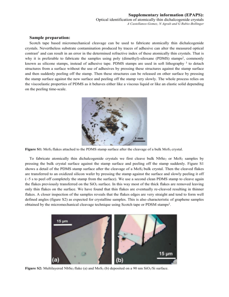
Supplementary information (EPAPS): Optical identification of atomically thin dichalcogenide crystals A Castellanos-Gomez, N Agraït and G Rubio-Bollinger Sample preparation: Scotch tape based micromechanical cleavage can be used to fabricate atomically thin dichalcogenide crystals. Nevertheless substrate contamination produced by traces of adhesive can alter the measured optical contrast1 and can result in an error in the determined refractive index of these atomically thin crystals. That is why it is preferable to fabricate the samples using poly (dimethyl)-siloxane (PDMS) stamps2, commonly known as silicone stamps, instead of adhesive tape. PDMS stamps are used in soft lithography 3 to detach structures from a surface without the use of adhesives by pressing these structures against the stamp surface and then suddenly peeling off the stamp. Then these structures can be released on other surface by pressing the stamp surface against the new surface and peeling off the stamp very slowly. The whole process relies on the viscoelastic properties of PDMS as it behaves either like a viscous liquid or like an elastic solid depending on the peeling time-scale. Figure S1: MoS2 flakes attached to the PDMS stamp surface after the cleavage of a bulk MoS 2 crystal. To fabricate atomically thin dichalcogenide crystals we first cleave bulk NbSe2 or MoS2 samples by pressing the bulk crystal surface against the stamp surface and peeling off the stamp suddenly. Figure S1 shows a detail of the PDMS stamp surface after the cleavage of a MoS2 bulk crystal. Then the cleaved flakes are transferred to an oxidized silicon wafer by pressing the stamp against the surface and slowly peeling it off (~5 s to peel off completely the stamp from the surface). We use a second clean PDMS stamp to cleave again the flakes previously transferred on the SiO2 surface. In this way most of the thick flakes are removed leaving only thin flakes on the surface. We have found that thin flakes are eventually re-cleaved resulting in thinner flakes. A closer inspection of the samples reveals that the flakes edges are very straight and tend to form well defined angles (figure S2) as expected for crystalline samples. This is also characteristic of graphene samples obtained by the micromechanical cleavage technique using Scotch tape or PDSM stamps2. Figure S2: Multilayered NbSe2 flake (a) and MoS2 (b) deposited on a 90 nm SiO2/Si surface. Supplementary information (EPAPS): Optical identification of atomically thin dichalcogenide crystals A Castellanos-Gomez, N Agraït and G Rubio-Bollinger Silicone stamps casting: The procedure to fabricate the silicone stamps in a reproducible way is the following: 1. We use a Teflon mold to cast the silicone stamps into an easy to handle shape (figure S3a). 2. Press the mold against a clean and flat surface like a glass slide or a silicon chip. Note that the part of the stamp used to cleave the crystals is the one in contact with this flat and clean surface (working surface). 3. Mix the 184 Sylgard polymer base and the curing agent in a 10:1 ratio by weight. 4. Pour the mixed 184 Sylgard into the mold. 5. Place the filled mold in a low vacuum chamber (500 mbar during 1 hour) to degas the mixed 184 Sylgard. In this way air bubbles are removed and the working surface of the stamp will be flat. 6. Place the filled mold in an oven at 60 ºC during 24 hours. 7. Unmold the stamp. A mold of Teflon (figure S3a) facilitates the unmolding process and prevents from breaking the stamp. The resulting stamps are shown in figure S3b. Figure S3. (a) Schematic of the mold/surface assembly used in the casting procedure. (b) Picture of two PDMS stamps fabricated using the described recipe. The one on the left shows NbSe2 flakes attached to its working surface. 1 2 3 M. Bruna and S. Borini, J. Phys. D: Appl. Phys. 42, 175307 (2009). M. Moreno-Moreno, A. Castellanos-Gomez, G. Rubio-Bollinger, J. Gomez-Herrero, and N. Agraït, Small 5 (8), 924-927 (2009). M. A. Meitl, Z. T. Zhu, V. Kumar, K. J. Lee, X. Feng, Y. Y. Huang, I. Adesida, R. G. Nuzzo, and J. A. Rogers, Nature Materials 5 (1), 33-38 (2006).

