AI LOOK OVER HARDWARE DESIGN – AGENT WITH STATE
advertisement
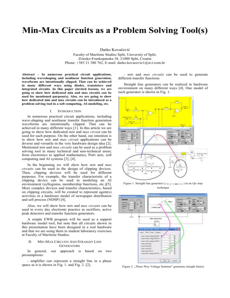
Min-Max Circuits as a Problem Solving Tool(s) Darko Kovačević Faculty of Maritime Studies Split, University of Split, Zrinsko-Frankopanska 38, 21000 Split, Croatia Phone: +385 21 380 762, E-mail: darko.kovacevic1@st.t-com.hr Abstract – In numerous practical circuit applications, including waveshaping and nonlinear function generation, waveforms are intentionally clipped. That can be achieved in many different ways using diodes, transistors and integrated circuits. In this paper (invited lesson), we are going to show how dedicated min and max circuits can be used for mentioned purpose(s). Also, we are going to show how dedicated min and max circuits can be introduced as a problem solving tool in a soft computing, AI-modeling, etc. I. - min and max circuits can be used to generate different transfer functions Straight line generators can be realized in hardware environment on many different ways [4]. One model of such generator is shown in Fig. 1. INTRODUCTION In numerous practical circuit applications, including wave-shaping and nonlinear transfer function generation waveforms are intentionally clipped. That can be achieved in many different ways [1]. In this article we are going to show how dedicated min and max circuit can be used for such purpose. On the other hand, our intention is to show how min and max circuit applications can be diverse and versatile in the very hardware design idea [2]. Mentioned min and max circuits can be used as a problem solving tool in many technical and non-technical areas; from electronics to applied mathematics, Petri nets, soft computing and AI systems [3], [4]. In the beginning we will show how min and max circuits can be used in the design of clipping devices. Then, clipping devices will be used for different purposes. For example, the transfer characteristic of a clipping device can be used in modeling an AI environment (syllogisms, membership functions, etc.)[5]. More complex devices and transfer characteristics, based on clipping circuits, will be created to represent agent(s) activities in a hardware model of newspaper distribution and sell process (NDSP) [4]. Figure 1. Straight line generator ( l y mx c ) in an Op-Amp technique Also, we will show how min and max circuits can be used in every day electronic practice as rectifiers, active peak detectors and transfer function generators. A simple EWB program will be used as a support hardware model tool, but note that all circuits shown in this presentation have been designed in a real hardware and that we are using them in student laboratory exercises at Faculty of Maritime Studies. II. MIN-MAX CIRCUITS AND STRAIGHT LINE GENERATORS In general, presumptions: our approach is based on two - amplifier can represent a straight line in a phase space as it is shown in Fig. 1. and Fig. 2. [2]. Figure 2. „Three-Way Voltage Summer“ generates straight line(s) A variety of min and max circuits performing corresponding set operations (see Fig. 3.) can be found in literature [5], but in the most of our applications we will use our original circuits (see Fig. 4. and Fig. 5.) based on standard operational amplifiers [6]. A. Min and Max Circuits Min and max circuits as a problem solving tool rely, on a mathematical theory of max (min) algebra [7], [8], [9], [10], and [11]. B. Min Circuit Definition. Assume A and B are two fuzzy subsets of X. Their intersection is a fuzzy subset D of X, denoted D A B (see Fig. 3. for illustration), such that for each x X Dx min Ax, Bx Ax Bx (1) It is common practice in the soft computing (fuzzy logic) literature to use symbol as the min operator. The operation min can be written in algebraic form that is convenient for hardware implementation [4]: min a, b (a b) a b / 2 (2) Using relation (2) we can design a min circuit in Op-Amp environment as it is shown in Fig. 4. Figure 3. Fuzzy set intersection or fuzzy logic AND-function C. Max circuit Definition. Assume A and B are two fuzzy subsets of X. Their intersection is a fuzzy subset C of X, denoted C A B , such that for each x X Cx max Ax, Bx Ax Bx (3) It is common practice in the soft computing (fuzzy logic) literature to use symbol as the max operator. The operation max can be written in algebraic form: max a, b a b a b / 2 (4) Using relation (4) we can design a max circuit in OPAmp environment as it is shown in Fig. 5. Figure 4. Min circuit in Op-Amp technique along with its „static“ and „dynamic“ responses to applied inputs. Note that Op-Amps (see Fig. 1.) were used to generate lines p1 and p2 to get “dynamic” response in a phase plain Figure 5. Min circuit in Op-Amp technique along with its „static“ and „dynamic“ responses to applied inputs. Note that EWB Op-Amps were used to generate lines p1 and p2 (“dynamic” response) III. MIN (MAX) CIRCUIT OPERATIVE EXTENSIONS A “better” look over min (max) circuit designed OpAmp technique gives us an opportunity to reconsider about additional facilities of that circuit; min/max function exchange can be easily established and new outputs give that circuit extra applicability (see Fig. 6.) A. Positive and negative clipping Clipping can be recognized as an undesirable result of overdriving an amplifier, i.e. any attempt to push an output voltage beyond the limits through which it can “swing” causes the tops and/or bottoms of a waveform to be “clipped” off. However, in numerous practical applications, including waveshaping and nonlinear function generation, waveforms are intentionally clipped [1]. Clipping as a notion can be introduced in the design of AI-algorithms [4]. Most often, the diodes along with reference batteries (voltage) are used to select for transmission a part of a waveform which lies above or below some reference voltage level. In some applications diodes are combined with operational amplifier(s) to obtain precision limiting circuits [1]. In this paper a somewhat different approach (a functional approach) to clipping actions is described. The approach is based on “standard” min and max circuits in “functional combination” with operational amplifiers that “play a geometric role” in the design of a desired transfer function [2] [3] [4]. Figure 6. Min (max) circuit designed in Op-Amp technique can have additional features; easy switching between min and max function, difference absolute value output, etc. Now, instead of using biased diodes, clipping can be accomplished by designing a desired transfer characteristic of a clipping device. Min and max circuits are used to combine linear transfer characteristics of operational amplifiers in a design of a nonlinear transfer characteristic of a certain clipping circuit. In that manner it is easy to design and mathematically describe a circuit transfer function of: - positive clipping circuit - negative clipping circuit - positive and negative clipping circuit - negative peak pass circuit - positive peak pass circuit If we take EB 0 then the transfer characteristic of a positive and negative clipping device can be used to represent a fuzzy set of “departures from zero”. B. Positive clipping If a sinusoidal waveform is to be clipped on a certain positive level (see Fig. 7.), two straight lines (amplifiers) have to be combined in a phase plain along with min circuit function to design desired transfer function G . Horizontal line l1 v0 represents clipping level ( v0 EB ) while the line l2 vo m vi c outside of clipping level, having a slope m 1 and c 0 , represents a linear region of a device (unity gain region). In that case the transfer characteristic of the clipping device can be formally represented as: G min( l1 , l2 ) It is obvious (see relation (5)) that lines “inputs” of a min circuit. (5) l1 and l2 are Figure 8. Negative clipping The transfer characteristic of the clipping device can be now formally represented as: G max( l1 , l2 ) (6) In this case lines l1 and l2 are “inputs” of a max circuit (see relation (6)). D. Positive and negative clipping Positive and negative clipping device is a min-max combination (see Fig. 9.), as its transfer function G can be expressed as: G min( Eb , max( Eb , l )) (6) where l represents a straight line uout m uin with m 1 . Clipping levels can be regarded as time varying variables and such conditions in a clipping device can be modeled as it is shown in Fig.10. C. Negative clipping If a sinusoidal waveform is to be clipped on a certain negative level (see Fig. 8.), two straight lines (amplifiers) have to be combined in a phase plain along with max circuit function. Horizontal line l1 v0 represents clipping level ( vo EB ) while the line l2 vo m vi c outside of clipping level, having a slope m 1 and c 0 , represents a linear region of a device (unity gain region). Well specified (defined) lines (Op-Amps outputs) are applied to min and (or) max circuit inputs to achieve desired non-linear transfer characteristic. Figure 7. Positive clipping Figure 9. Positive and negative clipping device Figure 10. Positive and negative clipping device with time dependent (modulated) clipping levels. Clipping levels can be a subject of agent negotiations what can cause their changes in a certain time frame IV. AI APPLICATION OF A CLIPPING DEVICE Clipping devices showed before can be used in modeling so called four-part multiagent agent diagram shown in Fig.11. [4.]. Different transfer characteristics can represent different (re)actions of a wholesaler (agent) in the NDSP [4.]. Let say that the agent activities are explained by a set of rules: If operator’s order is too high, then impose a certain limitation to operator’s current order If operator’s order is a zero order, then according to a current publisher wish, impose a minimal order (so called “presence”)to an agency In this case agent activities can be modeled using a time dependent clipping device showed in Fig.9. One must know that order limitations as well as the “presence” are variable quantities, along a tourist season. The transfer characteristic of a wholesaler (agent) can be expressed using relation (7): W W G (k ) min( nmax (k ), max( nmin (k ), nO (k ))) Figure 11. Four-part multiagent diagram; wholesaler (agent) controls order(s) on an operator [4] (7) W where nmax ( k ) represents maximum permissible order for W an agency, nmin (k ) represents so called presence, i.e. minimal permanent order that must be distributed through an agency and nO (k ) is a local operator order for a k-day. Note that wholesaler (agent), for some reasons can impose restrictions (changes) on operator’s order(s) [4]. V. PEAK PASS DEVICES Somehow different kind of clipping action is introduced in so called peak pass devices (see Fig.12. and Fig.13.). Instead of the positive or negative peaks being chopped off, the device follows ( vout vin ) the input when signal is above or below a certain level. The transfer characteristics show that linear operation (input signal following) occurs only when certain signal levels are reached and that the output remains constant below those levels. Figure 12. Positive peak pass device; G max( EB , vin ) If we combine a straight line generator having vout vin with a battery (+EB) along with a max circuit then we are going to realize a positive peak pass device. Transfer characteristic of the device is shown in Fig. 12. When the output of a straight line generator ( vout vin ) and a battery (−EB) are applied to the inputs of a min circuit (see Fig. 13.) a negative peak pass device will result. Input and output waveforms along with a transfer characteristic of the device are shown in Fig. 13. VI. Figure 13. Negative peak pass device; G min( EB , vin ) HALF AND FULL WAVE RECTIFIERS The design of a half-wave rectifier in min-max-circuit technique is quite simple (see Fig. 14.). A sinusoidal voltage E sin t is applied to one input on of a max circuit while the other input of max circuit is grounded (switch S is open). Therefore, output voltage can be expressed as: vout (t ) max( E sin t ,0)) (8) A full-wave rectifier in min-max-circuit technique (see Fig. 14.) can be designed in many ways (see Fig. 14 and Fig. 15.)[4]. If we use a circuit shown in Fig. 14, then the voltage on its output can be expressed by relation: vout (t ) E sin t max( E sin t ) min( E sin t ) (9) VII. MIN-MAX CIRCUITS AS A DEDICATED PROBLEM SOLVING TOOL A. Solving (in)equalities Let say that we want to find an electronic graphical solution for: a) x 1 3 and b) x 1 3 Let us graph x 1 3 . We will start with the plot of x (see Fig. 17.). Figure 14. A combination of a half and a full wave rectifier in min-maxcircuit technique The plot of x have to be shifted to the left to make x 1 , as it is shown in Fig. 18. Now, the plot of x 1 has to be shifted down to make it x 1 3 0 (see Fig. 19.) to get final solution, i.e. x1 2 and x2 4 . In the second case ( x 1 3 ) we need to add one min circuit to the output of the circuit shown in Fig. 19., to get the set of solutions, i.e. numbers x whose distance to 1 is at least 3 (see Fig. 20.). Figure 15. vout min( vin ,vin ) A. D-operators By modifying the min/max clipping circuits, we can obtain a class of transfer characteristics called Doperators, i.e. “ideal diode” operators (see Fig. 16.). For switching purposes the “ideal diode” is one way switch that is open when the imposed voltage is of one polarity and closed when the polarity is opposite. The D-operator circuit is a voltage-to-voltage min (max) circuit that would have the same response as a circuit that used an “ideal diode” as a switching element (see Fig. 16.). Figure 16. D-operators generator; Combing input and output menu it is possible to generate transfer characteristics of four precision rectifiers; GD max( 0, vin ) , GD max( 0,vin ) , GD min( 0, vin ) 1 2 and GD min( 0,vin ) 4 3 Figure 17. Plot of Figure 18. Plot of x in a phase plain; x max( x, x) x is shifted left to make the plot of x 1 . Two Op-Amps are need for that graph translation; y uout max(( x 1),( x 1)) Fig. 19. One can see two solutions: x1 uin 4 or x2 uin 4 m1 m2 c1 1 and c2 1 p1 m1vin c1 p2 m2vin c2 Figure 22. Dead zone for where D. Membership function generator A fuzzy set may be represented by a membership function. This function gives the grade (degree) of membership within the set, of any element of the universe of discourse. Figure 20. Electronic solution for the inequality x 1 3 ; The membership function maps the elements of the universe on to numerical values in the interval [0,1]. Specially, (,4 2, ) B. Trigonometry Trigonometric identity, relating circular functions of sine and cosine, i.e. cos 2 x sin 2 x 1 can be interpreted in hardware min-max environment as a line having a unity length as it is shown in Fig. 21. C. Dead zone In a dead zone operation (see Fig. 22.), the output is typically a linear function of the input, except for a band that is insensitive to the input. For example, input vin , vout max( m2 vin c2 , min( m1vin c1 ,0)) Z ( x) : X 0,1 where Z (x) is the membership function of the fuzzy set Z in the universe in X. Membership function can have distinct shapes. The most popular is a „tent function“. A „tent“ function can be generated using min-max-circuit technique as it is illustrated in Fig. 23. (10) Figure 23. A „tent“ function (membership function) can be expressed as Figure 21. Basic trigonometric relation (identity) interpreted in min-max hardware environment; min(sin x, cos x)2 max(sin x, cos x)2 1 Z ( x) maks(0, min( p1, p2 )) where: p1 Z ( x) x 1 and p2 Z ( x) x 1 E. Nonlinear transfer function synthesis Previously we showed so called four-part multiagent diagram representing NDSP [4]. The main role in that multiagent system plays a local operator. His (her) activities in that agent society can be briefly described by a simple rule base (see Fig. 24. for graphic illustration): Rule No.1. If a current remnant is below the lower limit Rl .l . (k ) , then increase the current order Rule No.2. If a current remnant is between the lower limit Rl .l . (k ) and the upper limit Ru.l . (k ) , then do not change the current order Rule No.3. If a current remnant is over the upper limit Ru.l . (k ) , then increase the current order Rule No.4. If the current order has been changed, then change the current operator’s transfer characteristic (see Fig. 18.) Figure 24. Two implications can be recognized in operator's activities: r (k ) max( o(k ) b(k ),0) o(k 1) , o(k 1) OpG(k 1) Operator's reaction (Rule No.1. or Rule No.3.) is typically a linear function of the input what means that lines p+ and p− represent the reactive part of operator's transfer characteristic (OTC). Hardware modeling starts with characteristic line generating (see Fig. 25a.). Then max and min circuits are added to synthesize OTC (see Fig. 25b.). F. Min/max circuits as theorem provers Absolute value is any maping u from a domain D to the real numbers R satisfying four fundamental properties among which subadditivity u v u v can be proven using Op-Amp technique (see Fig. 26.). a)“premises“(rules); control rule base Rbase (k ) VIII. MIN & MAX CIRCUITS AS ELEMENTS OF A COMPLEX GATE (AGENT COORDINATION DETECTOR) One of the major problems that arise in cooperative activity in NDSP is that of inconsistencies between local operator (agent) and inspector [4]. Wholesaler agent must establish negotiation platform once when two simultaneous, equal or unequal orders are detected in the ordering process and in the case when both expected orders are missing. In the hardware model of NDSP, an “exclusive OR gate” based on min-max-Op-Amp technique (see Fig. 27.) can be used for that purpose. The circuit will deliver zero output voltage as indication (trigger) that two non-zero orders are present simultaneously. In the case when nA nB 0 , the same coordination mechanism is going to be triggered again as the output of the gate Y 0 (see gate dynamics shown in Fig. 28.). Note than comparators used in the design of the “exclusive OR gate” are designed in min-max-Op-Amp technique as it is shown in Fig. 29. Three “input lines” are combined on min-max functions platform to design a complex circuit having “standard” comparator transfer characteristic (see Fig. 29.). b)“conclusion“; transfer characteristic of an operator synthesizes existing control rule base Figure 25. Hardware model of the control rule base is based on a single rule: If a control rule base about distribution and sale of a newspaper exists then it is possible to transform that rule base in a nonlinear transfer characteristic of an operator OG (k ) , i.e. O G(k ) maks(0, min( p (k ), max( p 0 (k ), p (k )))) Figure 26. In the A-area, y-coordinates of lines p1 and p2 are of opposite signs making subtracted response (to inputs) positive; inequality y y y y holds 1 2 1 Figure 27. “Exclusive OR gate” can serve as a coordination detector; if two orders 2 nA 0 and nB 0 , from two agent are imposed simultaneously, then a kind of coordination mechanism must be established to solve the emergent problem. Figure 29. Min-max comparator (“m-m-komp”); Figure 28. Simulation of the “exclusive OR gate” dynamic response uout max( U L , min( U H , p0 )) m where p0 uout m uin and IX. CONCLUSION In this paper (lesson) we have presented only of a part of min-max applications that have been developed in the electronic laboratory of Maritime faculty Split as it can be seen from the list below: - - - - original min and max circuits min-max clipping o positive clipping circuit o negative clipping circuit o positive and negative clipping circuit o negative peak pass circuit o positive peak pass circuit o inverted positive and negative clipping circuit D-operators four-part multiagent diagram half wave and full wave rectifiers clamping circuits nonlinear transfer function synthesis membership function generator(s) zero crossing detector active peak detector simple sort complex sort AI algorithm(s) o human activity hardware models o hardware models of coordination in a multiagent society min-max circuits in digital environment min-max circuits in mathematical environment o inequality solving tool o theorem solving (proving) tool o trigonometry solving tool o phase plain partition small expert systems hardware models of syllogisms Shown applications are marked (bold). In this presentation “painted applications” have been presented partly (“blue ones”), while “red ones” (in italic) are still waiting to be present in a future. In our opinion future work has to go in two directions; - more practical applications that can be used in electronic practice and production development of new AI algorithms in the field of coordination At the very end, it is possible to conclude that minmax circuits coming out from our laboratory may have a very perspective future as a problem solving tool in a different technical areas. ACKNOWLEDGMENT The results presented in this paper have been derived from the scientific research project: "New Technologies in Diagnosis and Control of Marine Propulsion Systems" supported by the Ministry of Science, Education and Sports of the Republic of Croatia. REFERENCES [1] Theodore F. Bogart, Jr., Electronic Devices and Circuits, PrenticeHall, Inc., Upper Saddle River, New Jersey, USA, 1997, pp.696707. [2] D. Kovačević et al, MIN and MAX Circuit Applications; Function Fitter, MIPRO 2010, 33rd International Convention on Information and Communication Technology, Electronics and Microelectronics, May 24-28, 2010, Opatija, Croatia, pp. 181-186. [3] D. Kovačević, A. Kovačević, N. Pribačić, Electronics In Mathematics; Idea About a Different Lesson in a Different Classroom, 10th International Educational Technology Conference, Proceedings Book Volume 1, Istanbul, Turkey, May 2010, pp. 496-501. [4] D. Kovačević, Hardware Modeling of Newspaper Distribution and Sell Process Control Based on Intelligent Agent Network Realization, PhD Thesis, Faculty of Electrical Engineering, Mechanical Engineering, and Naval Architecture, University of Split, Split, Croatia, July, 2012. [5] D. Kovačević, Sklopovske realizacije elemenata i funkcija teorije neizrazitih skupova, Magistarski rad, FESB – Split, listopad 1992. [6] D. Kovačević, A. Kovačević, Fuzzy Logic Controller Based on Standard Operational Amplifiers in Fuzzy Logic, Edited by J.F. Baldwin, John Wiley & Sons, Chichester, England, 1996., pp. 231-244. [7] en.wikipedia.org/wiki/Max-plus algebra, Max Plus Algebra [8] P. Butkovič, Max-algebra: the linear algebra of combinatorics, Linear algebra and its applications 367, Elsevier, Holland, 2003, pp. 313-335. [9] en.wikipedia.org/wiki/tropical_geometry, Tropical Geometry, 11.3.2012. [10] M. Gavalec, Computing matrix period in max-min algebra, Discrete Applied Mathematics, Volume 75, Issue 1, May 16, 1997, pp. 63-70. [11] S. Kurepa, Uvod u matematiku, Tehnička Knjiga Zagreb, Croatia, May 1975, pp. 109-140.
