IV. Radiation Damage - Gruner Group
advertisement
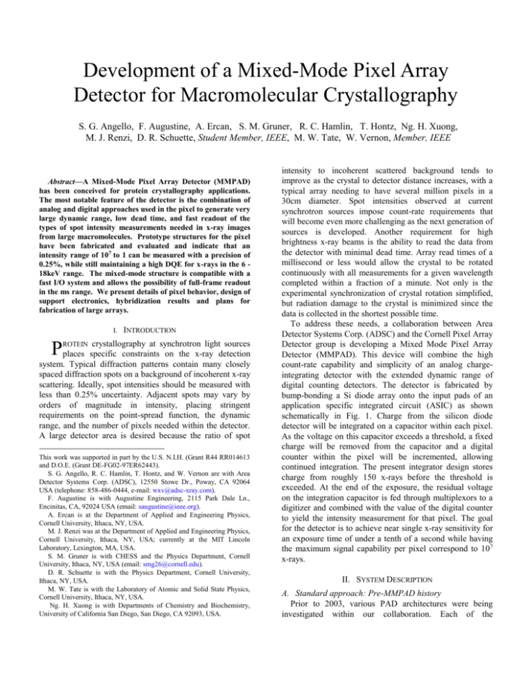
Development of a Mixed-Mode Pixel Array Detector for Macromolecular Crystallography S. G. Angello, F. Augustine, A. Ercan, S. M. Gruner, R. C. Hamlin, T. Hontz, Ng. H. Xuong, M. J. Renzi, D. R. Schuette, Student Member, IEEE, M. W. Tate, W. Vernon, Member, IEEE Abstract—A Mixed-Mode Pixel Array Detector (MMPAD) has been conceived for protein crystallography applications. The most notable feature of the detector is the combination of analog and digital approaches used in the pixel to generate very large dynamic range, low dead time, and fast readout of the types of spot intensity measurements needed in x-ray images from large macromolecules. Prototype structures for the pixel have been fabricated and evaluated and indicate that an intensity range of 107 to 1 can be measured with a precision of 0.25%, while still maintaining a high DQE for x-rays in the 6 18keV range. The mixed-mode structure is compatible with a fast I/O system and allows the possibility of full-frame readout in the ms range. We present details of pixel behavior, design of support electronics, hybridization results and plans for fabrication of large arrays. I. INTRODUCTION crystallography at synchrotron light sources Pplaces specific constraints on the x-ray detection ROTEIN system. Typical diffraction patterns contain many closely spaced diffraction spots on a background of incoherent x-ray scattering. Ideally, spot intensities should be measured with less than 0.25% uncertainty. Adjacent spots may vary by orders of magnitude in intensity, placing stringent requirements on the point-spread function, the dynamic range, and the number of pixels needed within the detector. A large detector area is desired because the ratio of spot This work was supported in part by the U.S. N.I.H. (Grant R44 RR014613 and D.O.E. (Grant DE-FG02-97ER62443). S. G. Angello, R. C. Hamlin, T. Hontz, and W. Vernon are with Area Detector Systems Corp. (ADSC), 12550 Stowe Dr., Poway, CA 92064 USA (telephone: 858-486-0444, e-mail: wxv@adsc-xray.com). F. Augustine is with Augustine Engineering, 2115 Park Dale Ln., Encinitas, CA, 92024 USA (email: saugustine@ieee.org). A. Ercan is at the Department of Applied and Engineering Physics, Cornell University, Ithaca, NY, USA. M. J. Renzi was at the Department of Applied and Engineering Physics, Cornell University, Ithaca, NY, USA; currently at the MIT Lincoln Laboratory, Lexington, MA, USA. S. M. Gruner is with CHESS and the Physics Department, Cornell University, Ithaca, NY, USA (email: smg26@cornell.edu). D. R. Schuette is with the Physics Department, Cornell University, Ithaca, NY, USA. M. W. Tate is with the Laboratory of Atomic and Solid State Physics, Cornell University, Ithaca, NY, USA. Ng. H. Xuong is with Departments of Chemistry and Biochemistry, University of California San Diego, San Diego, CA 92093, USA. intensity to incoherent scattered background tends to improve as the crystal to detector distance increases, with a typical array needing to have several million pixels in a 30cm diameter. Spot intensities observed at current synchrotron sources impose count-rate requirements that will become even more challenging as the next generation of sources is developed. Another requirement for high brightness x-ray beams is the ability to read the data from the detector with minimal dead time. Array read times of a millisecond or less would allow the crystal to be rotated continuously with all measurements for a given wavelength completed within a fraction of a minute. Not only is the experimental synchronization of crystal rotation simplified, but radiation damage to the crystal is minimized since the data is collected in the shortest possible time. To address these needs, a collaboration between Area Detector Systems Corp. (ADSC) and the Cornell Pixel Array Detector group is developing a Mixed Mode Pixel Array Detector (MMPAD). This device will combine the high count-rate capability and simplicity of an analog chargeintegrating detector with the extended dynamic range of digital counting detectors. The detector is fabricated by bump-bonding a Si diode array onto the input pads of an application specific integrated circuit (ASIC) as shown schematically in Fig. 1. Charge from the silicon diode detector will be integrated on a capacitor within each pixel. As the voltage on this capacitor exceeds a threshold, a fixed charge will be removed from the capacitor and a digital counter within the pixel will be incremented, allowing continued integration. The present integrator design stores charge from roughly 150 x-rays before the threshold is exceeded. At the end of the exposure, the residual voltage on the integration capacitor is fed through multiplexors to a digitizer and combined with the value of the digital counter to yield the intensity measurement for that pixel. The goal for the detector is to achieve near single x-ray sensitivity for an exposure time of under a tenth of a second while having the maximum signal capability per pixel correspond to 10 7 x-rays. II. SYSTEM DESCRIPTION A. Standard approach: Pre-MMPAD history Prior to 2003, various PAD architectures were being investigated within our collaboration. Each of the architectures was similar in that a Si diode array was bonded to an underlying ASIC. The Cornell PAD group built on their existing experience with charge-integrating (analog) pixels, whereas ADSC fabricated x-ray counting (digital) pixels. Fig. 1. Artist’s conception of an MMPAD detector. The bottom piece of the hybrid is the integrated circuit with an array of pixels and their pads that link to the top piece through the gold balls in the middle. The top piece is an array of silicon diodes where x-rays convert into charge that flows into the pads of the pixel array. The large pads in the foreground allow connection to external electronics. Both groups used 300 m thick silicon diode arrays fabricated by SINTEF as the x-ray detection layer. Tests have shown that the point-spread function in these devices is limited to the 150 m pixel size making them an excellent match to the diffraction problem at hand. Leakage currents were measured to be 4 pA/mm2 at room temperature. To test various bonding methods, half of the wafers had aluminum electrodes and the other half were triple metal coated, ending up with a gold external layer in order to simplify the assembly steps for bump bonding. Pulse height spectra from assembled detectors had an energy resolution of 1.0 keV FWHM for 5.9 keV x-rays. Observed leakage currents were dominated by edge effects outside of the active pixel array. The arrays became fully depleted for bias voltages less than 100 V. ADSC began by designing 16 x 16 pixel array circuits (digital type) in 2000, fabricating them in a 0.35 m process at Taiwan Semiconductor Manufacturing Corp. (TSMC). Chip design was done by Augustine Engineering and was based on a CERN chip (part of the Medipix project) [1], but with a counter that was 18 bits long. Tests from these fabrication runs showed several serious drawbacks to a purely digital counting approach. In the case of single x-ray counting, the analog input of the pixel is very sensitive to the transients generated within the ASIC, especially to the switching of the digital circuitry inside the pixel. Even if oscillation problems are eliminated through further development, the pulse shape changes that may occur can wreak havoc on the performance of the pixel. This kind of sensitivity also places restraints on how the diode array is bonded to the ASIC; increased input capacitance causes increased amplifier voltage gain. In addition to the digital-to-analog coupling problems, direct counting of x-rays has other difficulties. If a pixel does not have excellent x-ray sensitivity, i.e., both a low energy threshold and low noise contribution, then attempts to correct intensity measurements may fail because small changes in threshold can lead to significant changes in detection efficiency. Our goal for a detector is one that can measure the diffraction spot intensities with a precision of 0.25%, a goal that seems very difficult to obtain when pixelto-pixel sensitivity differences can cause losses of a significant fraction of the x-ray signal. Other generic problems with x-ray counting include speed limitations because the amplifier-shaper electronics must be bandwidth limited in order to avoid noise triggers. That limit is typically 1 MHz/pixel. Counting single x-rays also has the drawback of having to account for events where the charge from an x-ray event is split between two pixels. This is related to the previous threshold problem because small variations in threshold make it very difficult to avoid assigning the signal either to two pixels (double counting) or none (missing counts). Finally, the digital mode is very sensitive to edge breakdown of the silicon diode array; resulting noise pulses can simulate x-ray signals in many pixels at once. Concurrently, the Cornell group was continuing development of analog pixel array detectors [2]. Here charge generated within the detection diode is integrated onto a capacitor within the pixel. The voltage on the capacitor is digitized at the end of the exposure time and the integration capacitor is reset for the next frame. Again, 16 x 16 pixel arrays were fabricated, this time using a 0.25 TSMC process with a metal over metal capacitor option. The technology is reasonably mature and it doesn’t suffer from the count rate limitations or problems associated with charge sharing between pixels as with the digital counters. In addition the integration acts as a low-pass filter, making this method less susceptible to transients within the array. The main limitation is the single frame dynamic range owing to the limited charge storage capacity on the integration stage. One can increase the maximum stored signal by a small factor, but there is a limit to the size of capacitors that will fit in the 150 x 150 m2 pixel. The operating voltages within the ASIC are constrained, which in turn limits the stored charge. Deep submicron processes that are used because of their resistance to radiation damage are restricted to low voltages. B. Evolution of the Mixed Mode Given the problems of either a purely analog or digital approach, it became clear that another direction must be explored. In reality, each of the above approaches incorporates both analog and digital techniques within the ASIC. The photon-counting pixel relies on pulse shaping circuitry coupled with a threshold measurement to improve noise rejection in the analog domain. The integrating pixel contains multiplexing and reset logic. By changing the circuitry within the pixel, one can take advantage of key advantages of both approaches. Keeping the input integration stage of the analog approach retains the high count rate capability along with the immunity to charge sharing between pixels. Combining this with an in-pixel counter incremented by a threshold comparator gives the large dynamic range of a digital approach. A pixel block diagram is given in Fig. 2. floating point output by using a coarse resolution digital encoding, combined with a fine vernier analog measurement. The desired properties of the new detector are listed in Table 1. Note that a single exposure time of 0.1 sec would allow approximate single x-ray sensitivity as well as maximum possible flux of 107 x-rays at the high end; the dead time fraction would be 0.5%. TABLE I DESIGN GOALS FOR THE MIXED MODE DETECTOR Pixel Size Detector format ASIC Size Integrator well depth Digital overflow counter depth Overall well depth Maximum count rate Minimum count rate Readout Dead Time Systematic Error Limit X-ray Energy Range 150 x 150 m2 2048 x 2048 pixels 128 x 128 pixels 150 x-ray photons 262144 (218) 107 x-rays 108 x-rays/s < 10 x-rays/s < 0.5 ms 0.25% 5.9keV to 15keV III. PRELIMINARY TESTING Fig.2 Block diagram of a test pixel for the Mixed Mode PAD. External current is injected through the Tp1 connection. The internal current source can be varied with an external voltage. After a sufficient amount of charge is integrated, the comparator will trigger a digital count and charge removal from the integration node. Residual charge on the integration node can be sampled at the end of x-ray frame and is added to the value in the digital counter. This new approach is named ‘Mixed Mode’ to reflect the mixture of the analog (integration) and digital (counting) approaches to x-ray detection. It is not so named merely because the ASIC contains both analog and digital circuitry, since, as noted above, any of the PADs we have investigated meet this criteria. The Mixed Mode x-ray imaging detector began to evolve in the present PAD collaboration in 2002 at the suggestion of Sol Gruner [3]. The fundamental idea follows from the observation that calibration issues limit the absolute accuracy of all electronic detectors to, at best, a few tenths per cent. Conceptually, the experimenter requires an image consisting of an array of floating point numbers. Each number should have a mantissa good to a few tenths percent and an exponent big enough to span the range of intensities in the image. The MMPAD encompasses the equivalent of a Several methods for removal of charge from the integration stage have been prototyped and tested. One, a scheme in which a fixed charge is removed with each comparator pulse is described here. Tests were performed with a 50 fF integration capacitance with an 80 fC charge removal each time that the comparator fires. Since each xray generates on the order of 3000 electron-hole pairs, this corresponds to about 150 x-ray photons per comparator firing. The circuit can operate with input currents ranging from 80 fA (1 Hz firing rate) up to 80 nA (1 MHz firing rate) with excellent stability and linearity. One can illustrate the basic operation of the device by probing points within the pixel shown in Fig. 2. The point labeled Tp1 connects to the integrator input where the diode detector would be attached in a completed hybrid. An HP4145 current generator can inject currents between 1 pA and 100 nA into Tp1. Alternatively, the input pad can be left floating and an internal source used to inject current. The external source has the advantage of having a known current, but it suffers from excessive noise introduced by the probe. The internal source is a stable, low noise device but with unknown calibration. Probes can be connected to the integrator and the comparator at Tp2 and Tp3, respectively, with the results for two different input currents shown in Fig. 3. A scan of 250 points from the external current source is plotted in Fig. 4 along with the resulting frequency of the comparator pulses. Minimum current is 1 pA with the corresponding frequency of about 11 Hz, and maximum process that is currently being used should be radiation tolerant as well, but similar tests need to be performed. 105 Frequency (Hz) current is 69 nA with a frequency of 760 kHz. Low and high current regions are both limited by artifacts introduced by the external probe. Use of the internal source allows frequencies down to 1 Hz and up to 1 MHz. This measurement suggests that the desired dynamic range is within reach. The digital part should span 5 decades in intensity and the charge remaining on the integration node can be digitized to cover another 2 decades for a total range of 107:1 per pixel. 104 103 102 101 100 101 102 103 104 105 Current (pA) Fig.4 Frequency of the comparator pulses as a function of external current injection. Minimum current is 1 pA with the corresponding frequency of about 11 Hz and maximum current is 69 nA with a frequency of 760 kHz. V. HYBRID FABRICATION Fig. 3 Oscilloscope traces of voltage vs. time for the test points shown in Fig.2. Shown are integrator sawtooth (Tp2) and comparator pulses (Tp3). Input current to the integrator is generated by the internal source in the test pixel. Voltage scales are all 1 V/div. Signals are buffered through built-in isolation amplifiers in the test pixel. Time scale for (a) is 200 s/div, and the current is approximately 250 pA. The current in (b) is about 30 nA with a time scale of 1.00 s/div. IV. RADIATION DAMAGE At the start of the PAD project a major concern was whether the ASIC would be susceptible to radiation damage given the intense x-ray fluxes encountered at synchrotrons. Various test transistor structures were fabricated in the 0.35 m TSMC process and were subjected to x-ray doses of up to 50 Mrad. Structures laid out according to the CERN specs [4] (surrounding MOS devices with a ring) had no measurable effects at the maximum dose. CMOS n-channel transistors laid out in a standard linear configuration showed a detectable gate threshold shift at a dose of 30 Mrad. This damage threshold is still quite large. Since doses to the ASIC are expected to be on the order of 10 Mrad or less over the life of the detector, it was decided to forgo the ringgate layout at present, especially since this type of layout takes more area for a minimum size transistor. The 0.25 m Studies of the hybridization, or bump-bonding, of the silicon detector to an ASIC started in 2001 and several successful complete devices have been fabricated with the long established gold ball and conducting epoxy (GBCX) approach. Triple metallization, with gold as the last layer, was applied to the silicon diode array pads, and gold balls, about 70 m initial diameter were applied to the Al pads of the ASIC with a wire ball bonder. A flattening step makes the top of the balls flat and co-planar so that silver-bearing conductive epoxy can be applied in a simple and very reproducible fashion. The image in Fig. 5 shows a part of the 16 x 16 pixel array just after the epoxy has been applied, and the silver caps on the flattened gold balls are quite uniform. When this kind of ball/epoxy array is mated to the companion gold pads, a strong, clean connection is formed. Several other approaches for the hybridization are being evaluated, but have not yet been tested in a functional assembly. While the above method works well for small arrays, it might not be optimum for the larger devices with more than 104 connections. Ease of assembly, reliability and long-term stability should be considered. Additional bonding tests involving active pixel circuit elements placed under the bonding pads are also underway. At present, this area under the bump-bonding pads has been avoided because the effect of the ultrasonic wire bonding process that places the gold balls on the bonding pads is uncertain. Initial tests placing a chain of several hundred inverters under such pads found no defects after bonding. If further testing shows this area can be used reliably, then one has greater flexibility in the layout and functionality of the pixel. connections are built in. This example is an Altera FPGA, but a parallel effort is evaluating Xilinx FPGAs as well. A module in the detector will have a support board of the same size as the detector-ASIC hybrid, and the FPGA will support the ADC-multiplexor chips as well as take care of the digital data. Fig. 5. Close up of a portion of the detector chip. Each pad is 130 m on 150 m centers. The gold stud bumps are 80 to 100 m diameter. A flattening process developed at ADSC achieves coplanarity of +/- 2 m. The flattened bumps are then dipped into a tray of silver conducting epoxy. This image shows the silver epoxy on the gold balls. VI. FUTURE PLANS Fabrication is now underway of a 16 x 16 pixel array which will allow testing of the device in x-ray imaging. The pixel has been designed to allow correlated sample-and-hold functions that reduce the noise associated with resetting the integrator, but this remains to be tested. The goal for the detector is a 2048 x 2048 pixel array. Standard CMOS fabrication limits each ASIC to 128 x 128 pixels. Four ASICs would be bonded onto a single larger Si diode array, making a basic module. 64 such modules would be tiled together to make up the detector array. The relatively high data rates coming from the four chips of the module will be handled by a field programmable gate array (FPGA) that moves 32 high speed digital serial lines from the ASICs to short term memory at about 500 Mbyte/s. After the 0.5 ms readout time, the FPGA will move the data to the next level of the data collection pyramid at a more leisurely rate during data acquisition time of the next frame. The last stage of the data collection pyramid is a set of Ethernet cables going to a network switch; present planning calls for 16 cables of gigabit/s Ethernet to carry the approximately 0.12 Gigabit of data for each frame. Fig. 6 is a photograph of a prototype circuit that has an FPGA supporting several ASIC chips that plug in to the 44 pin and 84 pin carrier sockets. All communication with the board is by Ethernet, including the control patterns to the ASICs, and Mictor connectors for logic analyzer Fig. 6. The Altera based FPGA support element. There are six large sockets (84 pin) and two small (44 pin) for supporting a variety of ASICS in single and parallel combinations. Proms, in sets of three, define the properties of five different ASIC designs. VII. REFERENCES [1] M. Campbell, E. H. M. Heijne, G. Meddeler, E. Pernigotti, W. Snoeys, “A readout chip for a 64 x 64 pixel matrix with 15-bit single photon counting,” IEEE Trans. Nucl. Sci., vol. 45, no. 3, pp.751-753, June 1998. [2] M. J. Renzi, M. W. Tate, A. Ercan, S. M. Gruner, E. Fontes, C. F. Powell, A. G. MacPhee, S. Narayanan, J. Wang, Y. Yue and R. Cuenca, "Pixel array detectors for time resolved radiography (invited)", Review of Scientific Instruments, Volume 73, number 3, March 2002, 1621-1624. [3] A. Ercan, M. Renzi, M. Tate, S. Gruner, T. Hontz, “Recent analog xray pixel array detector developments,” Invited talk to the Eighth International Conference on Synchrotron Radiation Instrumentation (SRI 2003), San Francisco, CA, 25-29 August 2003. [4] G. M. Anelli, “Conception et cauterization de circuits integres resistnats aus radiations pour les detecteurs de particlules du LHC en technologies CMOS submicroniques profonds,” Microelectronique, Grenoble, France, Institut National Polytechnique de Grenoble, p214, 2000.
