電子工程系
advertisement
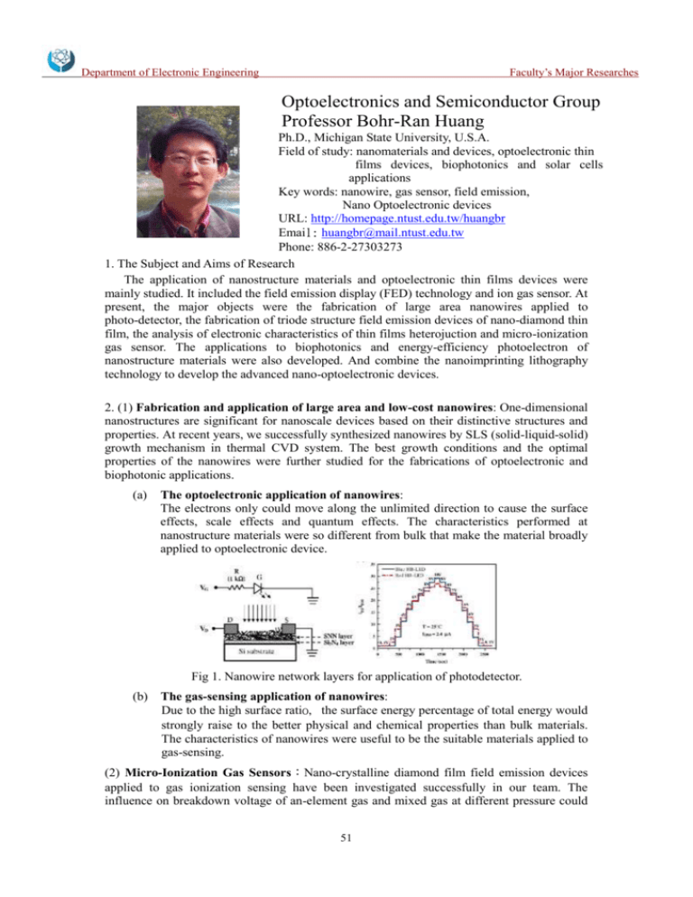
Faculty’s Major Researches Department of Electronic Engineering Optoelectronics and Semiconductor Group Professor Bohr-Ran Huang Ph.D., Michigan State University, U.S.A. Field of study: nanomaterials and devices, optoelectronic thin films devices, biophotonics and solar cells applications Key words: nanowire, gas sensor, field emission, Nano Optoelectronic devices URL: http://homepage.ntust.edu.tw/huangbr Email: huangbr@mail.ntust.edu.tw Phone: 886-2-27303273 1. The Subject and Aims of Research The application of nanostructure materials and optoelectronic thin films devices were mainly studied. It included the field emission display (FED) technology and ion gas sensor. At present, the major objects were the fabrication of large area nanowires applied to photo-detector, the fabrication of triode structure field emission devices of nano-diamond thin film, the analysis of electronic characteristics of thin films heterojuction and micro-ionization gas sensor. The applications to biophotonics and energy-efficiency photoelectron of nanostructure materials were also developed. And combine the nanoimprinting lithography technology to develop the advanced nano-optoelectronic devices. 2. (1) Fabrication and application of large area and low-cost nanowires: One-dimensional nanostructures are significant for nanoscale devices based on their distinctive structures and properties. At recent years, we successfully synthesized nanowires by SLS (solid-liquid-solid) growth mechanism in thermal CVD system. The best growth conditions and the optimal properties of the nanowires were further studied for the fabrications of optoelectronic and biophotonic applications. (a) The optoelectronic application of nanowires: The electrons only could move along the unlimited direction to cause the surface effects, scale effects and quantum effects. The characteristics performed at nanostructure materials were so different from bulk that make the material broadly applied to optoelectronic device. Fig 1. Nanowire network layers for application of photodetector. (b) The gas-sensing application of nanowires: Due to the high surface ratio, the surface energy percentage of total energy would strongly raise to the better physical and chemical properties than bulk materials. The characteristics of nanowires were useful to be the suitable materials applied to gas-sensing. (2) Micro-Ionization Gas Sensors:Nano-crystalline diamond film field emission devices applied to gas ionization sensing have been investigated successfully in our team. The influence on breakdown voltage of an-element gas and mixed gas at different pressure could 51 Faculty’s Major Researches Department of Electronic Engineering be observed to detect deadly gas in industrial factory. (3) Application of field emission properties by triode structure of nano-crystalline diamond films:Due to nano-crystalline diamond film have outstanding physical and chemical properties such as negative electron affinity. Therefore, nano-crystalline diamond film can be investigated for application as field emission electron sources. It was suggested that the triode structure of NCD films could improve the field emission characteristics. Fig 2. The triode structure of nanocrystalline diamond film. Fig 3. The SEM image of the gate structure for nanocrystalline diamond film. (4) Fabrication of nano thin film optoelectronic device by nanoimprinting lithography technology: The complex steps of traditional lithography technology cause the cost of process increased. Therefore, nanoimprinting lithography technology not only could replace traditional complex steps but also to minish the size of semiconductor device. At present, we use nanoimprinting lithography technology to develop the advanced nano-optoelectronic devices. 3. Selected Publications and Projects Publications: 1. Bohr-Ran Huang*, Jung-Fu Hsu, Chien-Sheng Huang, Yu-Tai Shih, and Kao-Sheng Lu, “Silicon nanowire networks for the application of field effect phototransistor”, Material Science and Engineering C,27, pp. 1197-1200, 2007. SCI, (Impact factor:1.325) 2. Ming-Shien Hu, Hsin-Li Chen, Ching-Hsing Shen, Lu-Sheng Hong, Bohr-Ran Huang, Kuei-Hsien Chen and Li-Chyong Chen, “Photosensitive gold nanoparticle-embedded dielectric nanowires”, Nature Materials, Vol. 5, pp. 102-106, 2006. SCI, (Impact factor:19.194) 3. Bohr-Ran Huang, Jung-Fu Hsu, Chien-Sheng Huang ,” The effects on the field emission properties of silicon nanowires by different pre-treatment techniques of Ni catalysts layers”, Diamond & Related Materials, Vol. 14, pp. 2105-8, 2005. SCI, (Impact factor:1.935) 4. B. R. Huang, C. S. Huang, C. F. Hsieh, Y. F. Liu, 2004, “The Electrical Conduction Mechanism of multiwalled carbon nanotubes film synthesized by microwave plasma chemical vapor deposition", Diamond & Related Materials. Vol. 13, pp. 2131-35. SCI, (Impact factor:1.935) 5. C. L. Li, B. R. Huang, S. Chattopadhyay*, L. C. Chen and K. H. Chen, 2004, “Amorphous boron carbon nitride as a pH sensor”, Applied Physics Letters, 84(15), pp.2676-78. SCI. (Impact factor: 3.977) Patents: (1) A METHOD FOR MASS PRODUCTION OF SILICON NANOWIRES (2) STRATIFIED SUBSTRATE STRUCTURE AND METHOD FOR PRODUCING NANOWIRES USING THE SAME Projects: (1) Bohr-Ran Huang, 2006-8, The Fabrication of nano-diamond Field Emission Display Array and its Application in Gas Sensors, National Science Council of the Republic of China. (2) Bohr-Ran Huang, 2007-2010, Large Area Fabrication and Optoelectronic Device Applications for Silicon Nanowires, National Science Council of the Republic of China. 52
