swastik-slot loaded microstrip antenna for c-band and x
advertisement

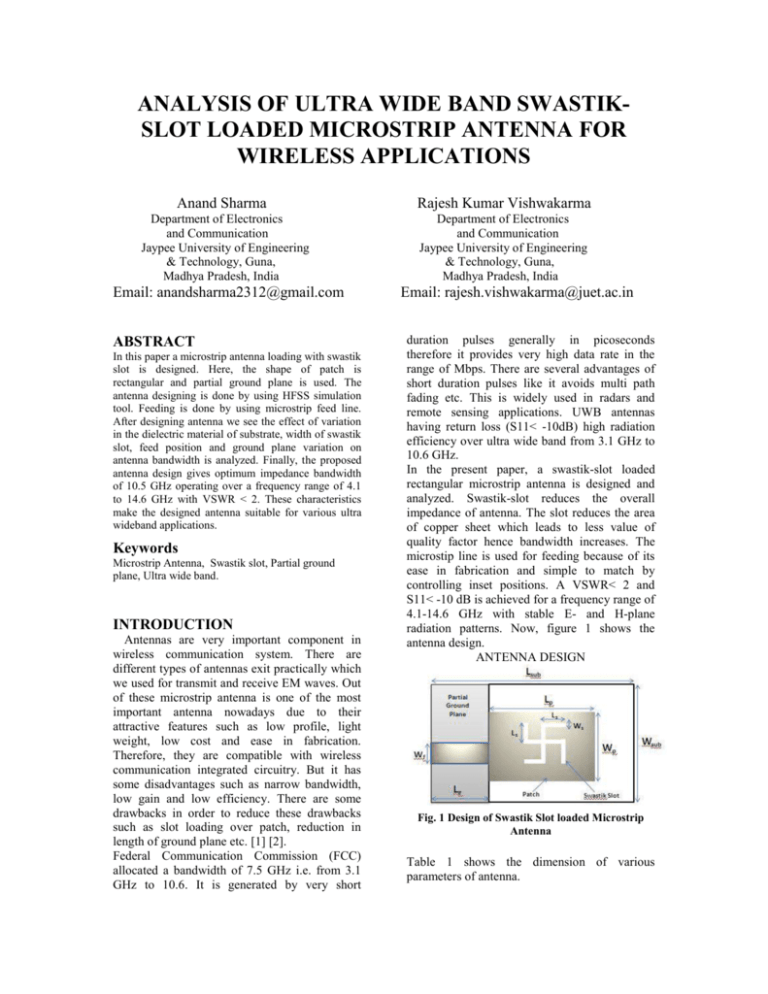
ANALYSIS OF ULTRA WIDE BAND SWASTIKSLOT LOADED MICROSTRIP ANTENNA FOR WIRELESS APPLICATIONS Anand Sharma Rajesh Kumar Vishwakarma Department of Electronics and Communication Jaypee University of Engineering & Technology, Guna, Madhya Pradesh, India Department of Electronics and Communication Jaypee University of Engineering & Technology, Guna, Madhya Pradesh, India Email: anandsharma2312@gmail.com ABSTRACT In this paper a microstrip antenna loading with swastik slot is designed. Here, the shape of patch is rectangular and partial ground plane is used. The antenna designing is done by using HFSS simulation tool. Feeding is done by using microstrip feed line. After designing antenna we see the effect of variation in the dielectric material of substrate, width of swastik slot, feed position and ground plane variation on antenna bandwidth is analyzed. Finally, the proposed antenna design gives optimum impedance bandwidth of 10.5 GHz operating over a frequency range of 4.1 to 14.6 GHz with VSWR < 2. These characteristics make the designed antenna suitable for various ultra wideband applications. Keywords Microstrip Antenna, Swastik slot, Partial ground plane, Ultra wide band. INTRODUCTION Antennas are very important component in wireless communication system. There are different types of antennas exit practically which we used for transmit and receive EM waves. Out of these microstrip antenna is one of the most important antenna nowadays due to their attractive features such as low profile, light weight, low cost and ease in fabrication. Therefore, they are compatible with wireless communication integrated circuitry. But it has some disadvantages such as narrow bandwidth, low gain and low efficiency. There are some drawbacks in order to reduce these drawbacks such as slot loading over patch, reduction in length of ground plane etc. [1] [2]. Federal Communication Commission (FCC) allocated a bandwidth of 7.5 GHz i.e. from 3.1 GHz to 10.6. It is generated by very short Email: rajesh.vishwakarma@juet.ac.in duration pulses generally in picoseconds therefore it provides very high data rate in the range of Mbps. There are several advantages of short duration pulses like it avoids multi path fading etc. This is widely used in radars and remote sensing applications. UWB antennas having return loss (S11< -10dB) high radiation efficiency over ultra wide band from 3.1 GHz to 10.6 GHz. In the present paper, a swastik-slot loaded rectangular microstrip antenna is designed and analyzed. Swastik-slot reduces the overall impedance of antenna. The slot reduces the area of copper sheet which leads to less value of quality factor hence bandwidth increases. The microstip line is used for feeding because of its ease in fabrication and simple to match by controlling inset positions. A VSWR< 2 and S11< -10 dB is achieved for a frequency range of 4.1-14.6 GHz with stable E- and H-plane radiation patterns. Now, figure 1 shows the antenna design. ANTENNA DESIGN Fig. 1 Design of Swastik Slot loaded Microstrip Antenna Table 1 shows the dimension of various parameters of antenna. (5) Table 1. Dimensions of Antenna S.No Parameters 1 Substrate 2 3 Rectangular patch Ground Plane 4 Swastik Slot 5 Feed line Dimensions Material Wsub=30 mm Lsub=30 mm Hsub= 1.6mm Lp= 16 mm Wp= 11.964mm Wg= 16 mm Lg= varying LHs= 5mm Lvs= 5mm Ws= 1.5mm Wf= 3.01mm Lf = 8 mm Varying Copper The width of microstrip line in microstrip antenna is given as follows: For Copper - Copper and for MATHEMATICAL FORMULATION Width of microstrip antenna is simply given as (1) Where, W= Width of Patch = Dielectric constant of the substrate Actual length of microstrip antenna is given as (2) Where, Where, A and B are given as follows = Effective length of the patch. = Extended electrical length Effective length of the patch is simply given by (3) Where, = Effective dielectric constant For low frequencies the effective dielectric constant is essentially constant. At intermediate frequencies its values begin to monotonically increase and eventually approach the values of dielectric constant of the substrate. Its value is given by, (4) h = thickness of the substrate In microstrip antenna, radiation occurs due to the fringing effects. Due to fringing effects electrical length of patch is greater than its physical length. This fringing depends on the width of patch and height of substrate [2].Now the extended electric length is given by ANTENNA DESIGN AND STRUCTURE In this paper, antenna is designed by using ANSOFT HFSS (High Frequency Structural Simulator) [4]. Method of finite element solver is used. Rectangular patch is 11.964 mm wide and 16 mm long. Dielectric material of substrate is varying and it is 30 mm wide and 30 mm long and height of the substrate is 1.6 mm. We take different types of substrate such as glass, FR4 epoxy, mica and Bakelite. Feeder position is varied at 1 mm, 1.5mm, 1.75 mm, 2mm, 2.25mm, 2.5mm and 2.75mm from the symmetrical position. . Ground plane is partial providing good impedance match with width 16 mm and varying length. At different lengths of partial ground plane i.e. 7mm, 7.5mm, 8mm, 8.5mm and 9mm, effect on antenna bandwidth is observed. Swastik-slot is used to decrease the overall impedance. It provides good impedance matching and higher bandwidth. XY Plot 7 dB(S(LumpPort1,LumpPort1)) -10.00 -20.00 Ws=4mm(Voilet) Ws=6mm(Blue) Ws=8mm(Green) -30.00 -40.00 -50.00 -60.00 2.00 4.00 6.00 8.00 10.00 12.00 14.00 Freq [GHz] 16.00 Curve Info Fig. 3 Return loss v/s frequency curve for varying width of swastik slot Table 3. Bandwidth at Different width of Swastik Slot HFSSDesign1 0.00 -10.00 Width of Swastik Slot (mm) 4 6 8 Range of Frequency (GHz) 4.24-14.7 4.17-14.2 4.07-13.5 Bandwidth (GHz) 10.46 10.03 9.43 Fractional Bandwidth (%) 145.2 139.3 130.9 -20.00 Lg=7mm(Violet) Lg=7.5mm (red) Lg=8mm(Blue) -30.00 Lg=8.5mm(Brow n) Lg=9mm (Green) -40.00 -50.00 2.00 4.00 6.00 8.00 10.00 12.00 Freq [GHz] 14.00 Curve Info Fig. 2 Return loss v/s frequency curve for varying length of ground plane Table 2. Bandwidth at Different Length of Ground Plane Length of Ground Plane (mm) 7 7.5 8 8.5 9 Range of Frequency (GHz) 4.24-14.7 4.24-14.13 4.17-14.2 8.4-13.8 8.5-10 Bandwidth (GHz) 10.6 9.89 10.03 5.4 1.5 Fractional Bandwidth (%) 147.2 137.36 139.30 75 20.83 16.00 From the figure 3 and table 3 it is clear that optimum bandwidth is achieved when width of swastik slot is 4 mm. Dielectric constant of the substrate also creates the effect on the bandwidth of microstrip antenna. So, now we see the effect of substrate material on bandwidth. Figure4 shows return loss v/s frequency curve at different substrate materials. XY Plot 12 Ansoft Corporation HFSSDesign1 0.00 -10.00 dB(S(LumpPort1,LumpPort1)) dB(S(LumpPort1,LumpPort1)) HFSSDesign1 0.00 The results shown here are simulated on HFSS software. In HFSS, rectangular patch and partial ground plane are made up of PEC (Perfect Electrical Conductor) and air or vacuum can be used for the radiation box. Firstly, the effect of varying length of partial ground plane on bandwidth of antenna is analyzed. Return loss gives us amount of power being reflected by the input port. For UWB antenna, return loss below -10 dB is considered to be quite efficient.Figure2 shows return loss v/s frequency curve at different length of ground plane. Ansoft Corporation XY Plot 1 Ansoft Corporation RESULTS AND DISCUSSION Mica(Red) Bakellite(Voilet) FR4(Blue) Glass(Green) -20.00 -30.00 -40.00 -50.00 2.00 4.00 6.00 8.00 10.00 12.00 14.00 Freq [GHz] From the figure 2 and table 2 it is clear that optimum bandwidth is achieved when length of ground plane is 8mm. Now, we see the effect of swastik slot width on bandwidth of antenna. Figure 3 shows return loss v/s frequency curve at different width of ground plane. 16.00 Curve Info Fig. 4 Return loss v/s frequency curve for varying dielectric constant Table 4. Bandwidth at Different Dielectric Material Substrate Material and Dielectric constant Mica (5.7) Glass (5.5) Bakelite (4.8) FR4 Epoxy (4.4) Range of Frequency (GHz) 3.8-12.11 3.9-12.3 4.11-13.17 4.2-14.1 Bandwidth (GHz) Fractional Bandwidth (%) 8.31 8.4 9.06 9.9 115.41 116.67 125.83 137.5 From the figure 4 and table 4 it is clear that optimum bandwidth is achieved when substrate is FR4 epoxy and its dielectric constant is 4.4. Finally, we see the effect of varying feeding position on the bandwidth of antenna. Figure 5 shows return loss v/s frequency curve at different feeding positions. XY Plot 18 Ansoft Corporation plane elevation plane with some particular azimuth angle φ is the principle E-plane. While for the x-y plane azimuth plane with some particular elevation angle θ is principle H-plane. Figure7 shows 2D E-plane radiation pattern at different frequencies with in the band 4.1-14.6 GHz. HFSSDesign1 0.00 Radiation Pattern 2 Ansoft Corporation HFSSDesign1 Curve Info 0 -30 dB(S(LumpPort1,LumpPort1)) -10.00 dB(GainTotal) Setup1 : LastAdaptive Freq='6GHz' Phi='0deg' 30 1.50 dB(GainTotal) Setup1 : LastAdaptive Freq='6GHz' Phi='90deg' -2.00 -60 60 -5.50 -20.00 -9.00 F=1.5mm(Red) F=1.75mm(Yellow ) F=2mm(Blue) F=2.25mm(Black) F=2.5mm(Green) F=2.75mm(Pink) -30.00 -90 90 -120 120 -40.00 -150 150 -180 -50.00 2.00 4.00 6.00 8.00 10.00 12.00 14.00 Freq [GHz] 16.00 Curve Info Fig. 5 Return loss v/s frequency curve for varying feeding position Fig.7a 2D E-plane Radiation Pattern at 6 GHz Radiation Pattern 3 Ansoft Corporation HFSSDesign1 Curve Info 0 -30 dB(GainTotal) Setup1 : LastAdaptive Freq='10GHz' Phi='0deg' 30 1.50 dB(GainTotal) Setup1 : LastAdaptive Freq='10GHz' Phi='90deg' -2.00 -60 60 -5.50 Table 5. Bandwidth at Different Feeding Positions -9.00 -90 Feeding position from symmetrical position (mm) 1.5 1.75 2 2.25 2.5 2.75 Range of Frequency (GHz) Bandwidth (GHz) Fractional Bandwidth (%) 90 -120 120 -150 150 -180 Fig.7b 2D E-plane Radiation Pattern at 10 GHz 4.4-13.5 4.4-13.6 4.3-13.7 4.2-13.7 4.2-14.1 4.2-14.53 9.1 9.2 9.4 9.5 9.9 10.33 126.38 127.78 130.55 131.94 137.5 143.47 Radiation Pattern 4 Ansoft Corporation HFSSDesign1 Curve Info 0 -30 1.50 60 -5.50 -9.00 -90 From the figure 5 and table 5 it is clear that optimum bandwidth is achieved when feeding position is 2.75mm from symmetrical position. we design antenna having ground plane length 8mm, swastik slot width 4mm, feeding position 2.75 mm from symmetrical position, substrate material is FR-4 epoxy. For this antenna design return loss is less than -10 dB in frequency range 4.1-14.6 GHz. Figure 6 shows return loss v/s frequency curve. XY Plot 3 dB(GainTotal) Setup1 : LastAdaptive Freq='12GHz' Phi='90deg' -2.00 -60 90 -120 Ansoft Corporation dB(GainTotal) Setup1 : LastAdaptive Freq='12GHz' Phi='0deg' 30 120 -150 150 -180 Fig.7c 2D E-plane Radiation Pattern at 12 GHz Figure8 shows 2D H-plane radiation pattern at different frequencies with in the band 4.1-14.6 GHz. Radiation Pattern 9 Ansoft Corporation HFSSDesign1 Curve Info 0 -30 dB(GainTotal) Setup1 : LastAdaptive Freq='6GHz' Theta='0deg' 30 1.00 dB(GainTotal) Setup1 : LastAdaptive Freq='6GHz' Theta='90deg' -3.00 -60 60 -7.00 -11.00 -90 90 HFSSDesign1 0.00 Curve Info dB(S(LumpPort1,LumpPort1)) Setup1 : Sw eep1 -5.00 dB(S(LumpPort1,LumpPort1)) -120 -10.00 -10.0689 120 -10.0677 -150 -15.00 150 -180 -20.00 Fig.8a 2D H-plane Radiation Pattern at 6 GHz -25.00 -30.00 2.00 4.00 6.00 8.00 10.00 12.00 14.00 16.00 Freq [GHz] Radiation Pattern 8 Ansoft Corporation MX1: 4.1871 MX2: 14.6070 HFSSDesign1 Curve Info 0 -30 dB(GainTotal) Setup1 : LastAdaptive Freq='10GHz' Theta='0deg' 30 5.00 Fig. 6 Return loss v/s frequency curve for optimum antenna design The E-plane is defined as the plane containing the electric field vector and the directions of maximum radiation while the H-plane is the plane containing the magnetic field vector and the direction of maximum radiation. The x-z dB(GainTotal) Setup1 : LastAdaptive Freq='10GHz' Theta='90deg' 0.00 -60 60 -5.00 -10.00 -90 90 -120 120 -150 150 -180 Fig.8b 2D H-plane Radiation Pattern at 10 GHz Radiation Pattern 6 Ansoft Corporation HFSSDesign1 Curve Info 0 -30 dB(GainTotal) Setup1 : LastAdaptive Freq='12GHz' Theta='0deg' 30 4.00 dB(GainTotal) Setup1 : LastAdaptive Freq='12GHz' Theta='90deg' -2.00 -60 60 -8.00 Engineering and Technology, Guna for his kind support and guidance and special thanks to Dr. Prashant Vasistha (Sc.’E’) Defense Lab, Jodhpur for his valuable suggestions. -14.00 -90 90 -120 120 -150 REFERENCES 150 -180 Fig.8c 2D H-plane Radiation Pattern at 12 GHz Figure9 shows 3D radiation pattern at different frequencies with in the band 4.1-14.6 GHz. Fig.9a 3D Radiation Pattern at 6 GHz Fig.9b 3D Radiation Pattern at 12 GHz CONCLUSION It is observed that swastik slot loaded microstrip antenna provided optimum bandwidth when length of partial ground plane is 8mm (4.17-14.2 GHz i.e 9.5 GHz), swastik slot width is 4mm (4.24-14.7 GHz i.e. 10.46 GHz), and feeding position is 2.75mm from symmetrical position (4.2-14.53 GHz i.e. 10.33 GHz). Finally, we saw the effect of dielectric material on bandwidth and got optimum bandwidth by using FR-4 epoxy substrate (4.2-14.1 GHz i.e. 9.9 GHz). Finally, we design antenna having ground plane length 8mm, swastik slot width 4mm, feeding position 2.75 mm from symmetrical position, substrate material is FR-4 epoxy then we get bandwidth (S11<-10 dB) 10.5 GHz ( 4.1-14.6 GHz). The proposed design of the antenna can be used for a variety of UWB applications including high speed data transfers, wireless connectivity between UWB-enabled devices and a variety of medical applications. ACKNOWLEDGMENT We would like to thank Prof. Rajiv Saxena (HOD E.C.E deptt.) Jaypee University of [1] Bahl I. J. & Bhartia P, Microstrip Antennas (Artech House, New Delhi), 1980. [2] Balanis C.A., Antenna Theory, Analysis and Design,(John Wiley, New York),1982. [3] FCC 1st Report and Order on Ultra Wideband Technology, Feb.2002. [4] Ansoft HFSS, Pittsburg PA 15219,USA. [5] Mohamed A. Hassanien and Ehab K.I. Hamad, ”Compact Rectangular U-Shaped Slot Microstrip Patch Antenna for UWB Applications”,2010 Middle East Conference on Antenna and Propagation, Cairo, Egypt. [6] J.A. Ansari, Anurag Mishra, Ashish Singh, ,”Analysis of Ultra-Wideband Patch Antenna for S,C & X Band Applications”, International Confrence on computer & Communication Technology(ICCCT)2011 [7] Guillanton, E., Dauvignac, J. Y., Pichot, C., & Cashman, J. (1998). A new design tapered slot antenna for ultrawideband applications. Microwave and Optical Technology Letters, 19(4), 286-289. [8] Qu, S. W., Ruan, C., & Wang, B. Z. “Bandwidth enhancement of wide-slot antenna fed by CPW and microstrip line”, IEEE Antennas and Wireless Propagation Letters, 5(1), 15-17 (2006). [9] Latif, S. I., Shafai, L., & Sharma, S. K. “Bandwidth enhancement and size reduction of microstrip slot antenna”, IEEE Transactions on Antennas and Propagation, 53(3), 994-1003 (2005). [10] J.A. Ansari, Anurag Mishra, Ashish Singh “Ultra Wideband Coplanar Microstrip Patch Antenna for Wireless Applications”, Wireless Pers Commun (2013)69:1365-1378 DOI 10.1007/s 11277-012-0638y


