11004_2302_r01
advertisement
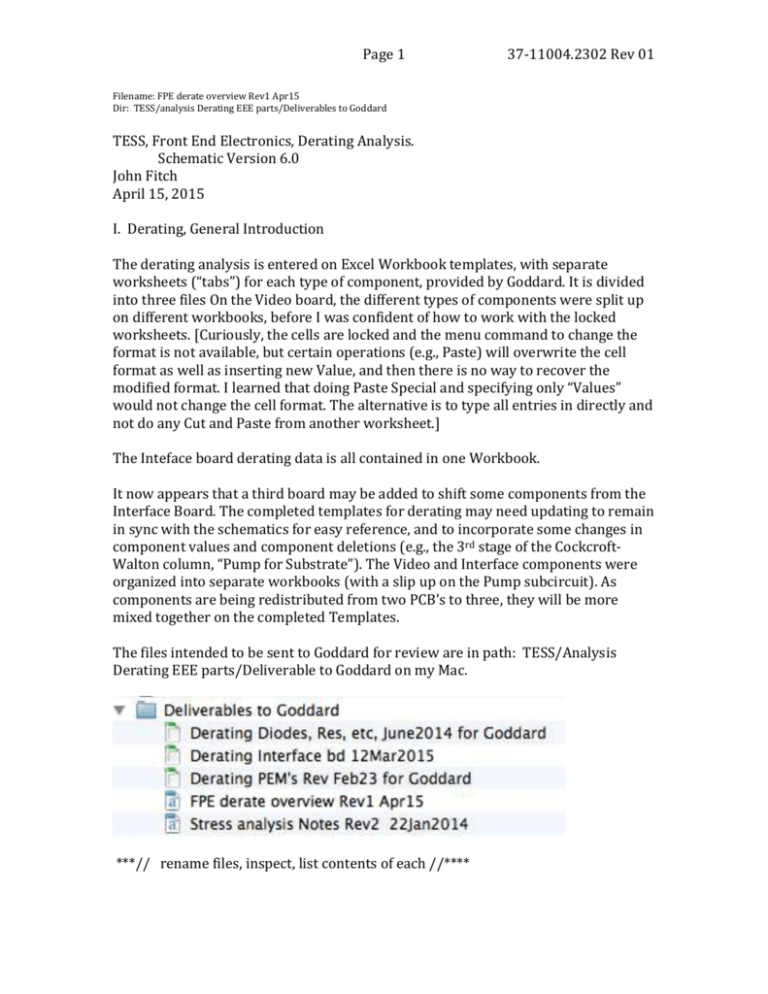
Page 1 37-11004.2302 Rev 01 Filename: FPE derate overview Rev1 Apr15 Dir: TESS/analysis Derating EEE parts/Deliverables to Goddard TESS, Front End Electronics, Derating Analysis. Schematic Version 6.0 John Fitch April 15, 2015 I. Derating, General Introduction The derating analysis is entered on Excel Workbook templates, with separate worksheets (“tabs”) for each type of component, provided by Goddard. It is divided into three files On the Video board, the different types of components were split up on different workbooks, before I was confident of how to work with the locked worksheets. [Curiously, the cells are locked and the menu command to change the format is not available, but certain operations (e.g., Paste) will overwrite the cell format as well as inserting new Value, and then there is no way to recover the modified format. I learned that doing Paste Special and specifying only “Values” would not change the cell format. The alternative is to type all entries in directly and not do any Cut and Paste from another worksheet.] The Inteface board derating data is all contained in one Workbook. It now appears that a third board may be added to shift some components from the Interface Board. The completed templates for derating may need updating to remain in sync with the schematics for easy reference, and to incorporate some changes in component values and component deletions (e.g., the 3rd stage of the CockcroftWalton column, “Pump for Substrate”). The Video and Interface components were organized into separate workbooks (with a slip up on the Pump subcircuit). As components are being redistributed from two PCB’s to three, they will be more mixed together on the completed Templates. The files intended to be sent to Goddard for review are in path: TESS/Analysis Derating EEE parts/Deliverable to Goddard on my Mac. ***// rename files, inspect, list contents of each //**** Page 2 37-11004.2302 Rev 01 II. Overview The block diagrams for the Focal Plane Electronics, Interface Board Assy and Video Board Assy, show the hierarchical structure of the schematics. The symbol for each subcircuit is a block containing a name which is a shortened up nickname of the Title of schematic of that subcircuit. The circuit partitioning is changing from 2 pcb’s to 3 pcb’s so reference designations may change (probably must change to accomodate the PCB software. The schematics are divided into separate file schematics for each hierarchical subcircuit, and one for the top level. Only the top level has plain vanilla reference designators. The reference designator for each instance (“instantiation” to sw people) of a subcircuit is Xn where n is 1,2,3... etc. The ref des for components in a subcircuit instance are the concatenation, Xn/C1 for example. Nested subcircuits result in Ref Des’s like X1/X5/X2/C1. The Video Board Assembly is/was one pcb containing the signal processing circuitry for the CCD’s outputs, and generates bias voltages for the CCD. The pulse train signals to drive the CCD gates to clock the CCD, are generated on the Interface board. The Interface Board Assembly is/was one pcb containing the Artix FPGA, ad the circuitry to drive the CCD gates and bias voltages. The filtering circuit for power from the DHU is evolving. As of this writing, analysis is underway of the transient response and possible ringing from the large step in supply current at the start and end of Frame Transfer. I did not include the tantalum capacitors that were expected to change. In the column Ref. Des. of the templates, I stripped the subcircuit prefixes from reference designators and give the board assy and subcircuit identification in the two following columns FGV and “Schematic”. The applicable Derating Requirements from EEE-INST-002 include: 1. Table 4 RESISTOR DERATING REQUIREMENTS a. Style RM, fixed, Film, Chip, ER 2. Table 4 CAPACITOR DERATING REQUIREMENTS a. Type Ceramic b. Type tantalum 3. Table 4 DERATING REQUIREMENTS FOR PEMs Page 3 37-11004.2302 Rev 01 4. Table 4 MICROCIRCUIT DERATING REQUIREMENTS [hermetic] 5. Table 4 TRANSISTOR DERATING REQUIREMENTS 6. Table 4 DIODE DERATING REQUIREMENTS a. General Purpose 7. There is also one crystal oscillator which has its own Derating Requirements. III. Derating analysis The derating analysis is carried out for the “worst case” normal operating condition of the circuit. The “worst case” means that if something is programmable by software, the full range of possible values that could be set must be considered, including those that would not intentionally be used under “normal operating conditions”. The rationale is that a software bugs may occur, and also the software can’t be expected to be constrained under all modes including testing, development and startup, to remain within the range that would be used for taking measurements. Failure modes where one or more components are failed are not considered. As of this writing, investigation and testing has concluded that no IC’s are susceptible to latchup. Many IC’s have a current limiting resistor in series with its Vcc line. Some of these circuits were right at the power limits of the resistors, and might be slightly exceeded assuming +5% tolerance on supply voltages and on what the voltage drop is across the latched-up IC. The templates now have values entered based on normal, non-latchedup operation. However, it should be noted most of the resistors were only slightly above a 60mW derated value, like 62 to 65mW, even at +5% supply tolerance and a conservative, low value for latched up IC drop. Some IC’s that were never thought vulnerable have only RC filtering on the VCC line to filter noise, e.g. 49.9 ohms, which was never intended to tolerate latchup. A. Resistors There are no resistors with more than a negligible power level in normal operation. Before obtaining the Goddard Excel Template for tabulating derating data and determining Pass/Fail, I first made up a spreadsheet and did a screen on resistors by first calculating the “critical value” of resistance for each of the major supply voltages for the lowest value of nominal resistor power rating, (0.1W, derating to 0.06W). The table for critical values appears to the top right of the spreadsheet, in a box border. This is the value that would put the power at the limit of 0.6 derating factor per Table 4. For 0.1W nominal power rating, derated by 0.6x, these are 24V 10k 15V 3750 12 2400 Page 4 5 37-11004.2302 Rev 01 417 There are few resistors where even a cursory examination of power dissipation is needed. IV. Derating Templates The data is entered into templates provided by Goddard (Paula Pruessner paula.s.pruessner@nasa.gov 301-286-8809, via Chris Green). The Pass/Fail column incorporates formulas to automatically determine if the data entries result in passing or failing the derating requirements, and display a vivid RED “FAIL” entry or a soothing baby-blue “PASS”. Each component category from EEE-INST-002 has its own worksheet [and some categories are subdivided into two worksheets, e.g. analog and digital microcircuits]. The various worksheets have slightly different formats. Thermal calculations are handled differently. PEM’s have a cell to enter the board temperature and uses this as an ambient temperature to calculate temperature rise, and some worksheets have the operating temperature entered as data. IV. Workbook contents Derating Video Bd Vol1 June2014.xls Resistors General Purpose Diodes Digital Microcircuits – PEM Junction Transistors Derating Video Bd Vol2 Feb23.xls Microcircuit – Hermetic (LM195) Digital Microcircuits – PEM Lin – Mixed Microcircuit - PEM Derating Video Bd IC’s Rev Feb23.xls Microcircuit – Hermetic (LM195) Digital Microcircuits – PEM Lin – Mixed Microcircuit - PEM Derating Interface Bd 1Mar2015.xls Capacitors Resistors General Purpose diodes Microcircuit – hermetic [Digital Microcircuits – PEM none!! Double-check?] Lin-Mixed Microcircuit – PEM Crystal Oscillator Page 5 Junction Transistors MOSFET Transistors (empty, add Q3 & 4 Booster) 37-11004.2302 Rev 01
