Test Results for an Array-Based GM-APD Detector Before and After
advertisement
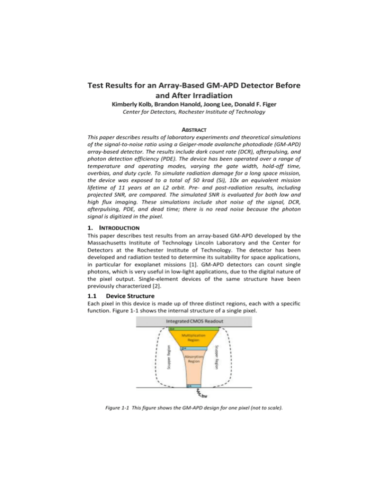
Test Results for an Array-Based GM-APD Detector Before and After Irradiation Kimberly Kolb, Brandon Hanold, Joong Lee, Donald F. Figer Center for Detectors, Rochester Institute of Technology ABSTRACT This paper describes results of laboratory experiments and theoretical simulations of the signal-to-noise ratio using a Geiger-mode avalanche photodiode (GM-APD) array-based detector. The results include dark count rate (DCR), afterpulsing, and photon detection efficiency (PDE). The device has been operated over a range of temperature and operating modes, varying the gate width, hold-off time, overbias, and duty cycle. To simulate radiation damage for a long space mission, the device was exposed to a total of 50 krad (Si), 10x an equivalent mission lifetime of 11 years at an L2 orbit. Pre- and post-radiation results, including projected SNR, are compared. The simulated SNR is evaluated for both low and high flux imaging. These simulations include shot noise of the signal, DCR, afterpulsing, PDE, and dead time; there is no read noise because the photon signal is digitized in the pixel. 1. INTRODUCTION This paper describes test results from an array-based GM-APD developed by the Massachusetts Institute of Technology Lincoln Laboratory and the Center for Detectors at the Rochester Institute of Technology. The detector has been developed and radiation tested to determine its suitability for space applications, in particular for exoplanet missions [1]. GM-APD detectors can count single photons, which is very useful in low-light applications, due to the digital nature of the pixel output. Single-element devices of the same structure have been previously characterized [2]. 1.1 Device Structure Each pixel in this device is made up of three distinct regions, each with a specific function. Figure 1-1 shows the internal structure of a single pixel. Figure 1-1 This figure shows the GM-APD design for one pixel (not to scale). The absorber depletion region has a medium-strength electric field that moves carriers to the multiplier region, which has a strong electric field (above breakdown voltage) to facilitate avalanches. A weak electric field, called a “scupper,” surrounds the absorption and multiplication regions of each pixel to direct carriers generated outside of these regions to the cathode without initiating an avalanche, reducing the dark count rate [3]. 1.2 Device Operation A GM-APD exposure is comprised of many individual detection cycles, each of which contains three main signals. At the start of the cycle, an arm pulse is asserted to set the reverse bias across the diodes above the breakdown voltage. The voltage is kept high for a short period of time (generally on the order of 0.1 μs), after which an individual pixel may or may not avalanche. In the event of an avalanche, the quenching circuit detects an increase in current and actively sets the voltage below the breakdown voltage, or disarms the pixel, to stop the avalanche. At the end of the gate (the time that the voltage is allowed to be high), the pixel state is recorded, a “one” or “zero,” corresponding to whether the pixel experienced an avalanche. After the state is recorded, the pixels are actively disarmed, regardless of state, and after a specified delay (the hold-off time) the pixel is armed again. The output of a pixel from a given exposure is the total number of avalanches recorded. The ratio of avalanches to number of gates is the avalanche probability, from which the flux can be estimated. Since this estimation method is fundamentally different from that used for CCD or CMOS detectors, the form of the expression for the signal-to-noise ratio (SNR) is fundamentally different, as well. For the detector discussed here, the dominant noise characteristics for SNR are determined by dark count rate (DCR), afterpulsing probability, and photon detection efficiency (PDE). DCR and PDE are analogous to dark current and QE, but DCR and PDE values include the avalanche initiation probability, which degrades the device’s ability to detect a carrier when it is less than 1 [4]. 2. PRE-RADIATION RESULTS The performance of detectors in space degrades over time due to absorption of high energy radiation. Damage in the lattice structure of the semiconductor eventually leads to higher dark current and trap density, both decreasing SNR. The extent to which lattice damage affects the performance of a detector is determined by the internal structure and operation of the device. The GM-APD array-based detector presented here was irradiated to simulate the damage it would receive on a space mission. Since irradiation is permanently destructive, thorough characterization of the device prior to irradiation was extremely important. The full characterization suite included DCR, afterpulsing, PDE, persistent charge, intra-pixel sensitivity, and crosstalk. However, as mentioned above, only DCR, afterpulsing, and PDE are discussed. 2.1 Dark Count Rate (DCR) Dark count rate (DCR) is the rate at which electrons enter the multiplication region with sufficient avalanche initiation probability for triggering an avalanche. In order to calculate DCR for a GM-APD, a conversion must be made from the 2 raw data, which is the number of triggered gates, to an estimate of the electron signal in Hertz. First, the total number of avalanches is divided by the total number of frames to calculate the probability of an avalanche in a single frame or gate. Since the detector data is digital, there is no distinction between a gate in which five electrons entered the multiplication region and a gate in which only one electron did – in either case, only one avalanche can be recorded. However, since the rate at which electrons arrive at the multiplication region is Poissonian, the Poisson probability model can be used to solve for the mean electron arrival rate from the gate avalanche probability, given the gate length (in the case of zero afterpulsing). For the case of no incident radiation (a dark exposure): 𝑛𝑎𝑣𝑎𝑙𝑎𝑛𝑐ℎ𝑒𝑠 = 𝑃𝑎𝑣𝑎𝑙𝑎𝑛𝑐ℎ𝑒 = 1 − 𝑒 −𝜆𝑑 ∙𝑡𝑔𝑎𝑡𝑒 𝑛𝑔𝑎𝑡𝑒𝑠 𝜆̂𝑑 = −ln(1 − 𝑃𝑎𝑣𝑎𝑙𝑎𝑛𝑐ℎ𝑒 ) 𝑡𝑔𝑎𝑡𝑒 Eq. 1 Eq. 2 where λd is the number of electrons detected per second in the dark. Figure 2-1 shows measured DCR vs temperature. Two different arm periods are used to account for the increase in afterpulse probability at lower temperatures. Figure 2-1 Median DCR vs temperature is shown. The gate time was constant at 10 μs. The arm period was increased at lower temperatures to avoid significant afterpulsing. 2.2 Afterpulsing Afterpulsing is a phenomenon in which carriers are caught in “traps” for a random period of time and then released. This delayed release results in nonPoissonian noise that is dependent on the state of previous gates, since the majority of traps are populated during an avalanche. In a gated device, afterpulsing manifests as an increase in the measured DCR when compared to a measurement with no afterpulsing. Using a theoretical model for avalanche probability, the afterpulse probability at any setting can be determined, given a data point that has an afterpulsing probability of zero. 𝑃𝑎𝑣𝑎𝑙𝑎𝑛𝑐ℎ𝑒 = 1 − 𝑒 −𝜆𝑑 ∙𝑡𝑔𝑎𝑡𝑒 1 − 𝑝𝑎𝑓𝑡 𝑒 −𝜆𝑑 ∙𝑡𝑔𝑎𝑡𝑒 Eq. 3 3 ̂ 𝑝̂𝑎𝑓𝑡 = 1 − 𝑒 𝜆𝑑 ∙𝑡𝑔𝑎𝑡𝑒 (1 − 𝑃𝑎𝑣𝑎𝑙𝑎𝑛𝑐ℎ𝑒 ) 𝑃𝑎𝑣𝑎𝑙𝑎𝑛𝑐ℎ𝑒 Eq. 4 paft is defined here as the probability of one or more afterpulse carriers being present in the pixel during a gate (it includes avalanche initiation probability). Eq. 3 and Eq. 4 are derived using a careful representation of avalanche probability for each gate in a summation series and the Maclaurin series identity [5]. For this afterpulsing probability estimate to be valid, a few assumptions must be true. 1) The pixels are disarmed at the end of the gate and no avalanche events occur outside the gate window. 2) There is no (or insignificant) dependence on gates previous to the gate immediately prior to the gate of interest (i.e., the probability of an avalanche in the current gate is only a function of the state of the gate immediately before it and the photon and dark generation process). 3) There is no significant delayed crosstalk from neighboring pixels (i.e., afterpulsing occurs only as a result of the same pixel’s previous state, not a neighboring pixel’s previous state). Figure 2-2 shows the median afterpulse probability measured at each arm period value for various temperatures. By using the DCR at the longest arm period as the value for λd, and the observed avalanche probability at various arm period settings for P, the afterpulse probability paft can be calculated at each point. Figure 2-2 shows the median calculated afterpulsing probability vs hold-off time for various temperatures. Note that paft increases with decreasing temperature. Figure 2-2 Pre-radiation median afterpulsing probability vs arm period (hold-off time + gate time) is shown. The gate time was kept constant at 1 μs. The coldest temperature exhibited the highest afterpulsing probability. 2.3 Photon Detection Efficiency (PDE) Photon detection efficiency (PDE) is the ratio of electrons detected by the device to the number of photons incident on the device. The detector characterized here has a low-fill-factor design (Figure 1-1) and therefore its performance is not representative of what is expected for detectors optimized for imaging. The measured PDE values are not corrected for the very small active area of this device (~ 9% total pixel area). 4 A calibrated photodiode was used to measure the flux inside of an integrating sphere illuminated by a monochromator to determine the number of photons incident on the detector during the experiment. The calibration process used a detector substitution method, wherein two diodes simultaneously measured the flux at the integrating sphere and the detector plane to account for differences between the two locations. The ratio of photons between the two photodiodes at each wavelength corrected the raw PDE measurements. To calculate PDE, dark data was taken at each wavelength (to account for any wavelength-specific system light leakage) along with the illuminated frames. Both data sets were converted to electron flux from avalanche probability. The dark flux was subtracted from the illuminated flux to calculate the measured electron flux from photo-generation. Assuming paft = 0: 𝑃𝐷𝐸 ∙ 𝜆̂𝑝 = − ln(1 − 𝑃𝑎𝑣𝑎𝑙𝑎𝑛𝑐ℎ𝑒 ) − 𝜆̂𝑑 ∙ 𝑡𝑔𝑎𝑡𝑒 𝑡𝑔𝑎𝑡𝑒 Eq. 5 The photo-generated flux was then normalized by area and compared to the photon flux measured by the photodiode (corrected for dark current, area, sensitivity, and calibrated photon flux ratio) to find the % PDE at each pixel. The gate width was optimized for three separate regimes in order to maximize SNR. Since the electron flux calculation for the detector is normalized by the gate width (Eq. 5), there is no difference between results derived from experiments with different gate widths, aside from SNR. Based on extrapolated values for PDE and measured values for DCR, three gate widths were chosen to maximize the SNR at each wavelength. Figure 2-3 shows the PDE results vs wavelength. Figure 2-3 PDE vs wavelength of a representative pixel is shown. The gate time was varied to accommodate varying signal levels from the calibrated source for maximum sensitivity. 3. THEORETICAL SNR While an in-depth derivation of the SNR expression for the detector presented here is outside the scope of this paper, a brief overview of it is given. Eq. 6 gives the estimate of the number of photo-generated carriers when afterpulsing probability is not zero, taking PDE into account. 5 1 − 𝑃𝑎𝑣𝑎𝑙𝑎𝑛𝑐ℎ𝑒 − ln [ ] − 𝜆̂𝑑 ∙ 𝑡𝑔𝑎𝑡𝑒 1 − 𝑝𝑎𝑓𝑡 𝑃𝑎𝑣𝑎𝑙𝑎𝑛𝑐ℎ𝑒 ̂𝜆𝑝 = 𝑃𝐷𝐸 ∙ 𝑡𝑔𝑎𝑡𝑒 Eq. 6 Eq. 7 gives the SNR of the estimate, derived using the Markov Chain method [6]. 𝑃𝐷𝐸 ∙ 𝜆𝑝 ∙ 𝑡𝑔𝑎𝑡𝑒 ∙ 𝑛𝑔𝑎𝑡𝑒𝑠 𝑆𝑁𝑅 = √𝑃1 𝑃0 (1 + 2 𝑝𝑎𝑓𝑡 𝑒 −(𝑃𝐷𝐸∙𝜆𝑝 +𝜆𝑑 )𝑡𝑔𝑎𝑡𝑒 2 1 − 𝑝𝑎𝑓𝑡 )( ) 𝑛𝑔𝑎𝑡𝑒𝑠 −(𝑃𝐷𝐸∙𝜆𝑝 +𝜆𝑑 )𝑡𝑔𝑎𝑡𝑒 𝑃0 (1 − 𝑝𝑎𝑓𝑡 ∙ 𝑃1 ) 1 − 𝑝𝑎𝑓𝑡 𝑒 Eq. 7 where 𝑃1 = 1 − 𝑒 −(𝑃𝐷𝐸∙𝜆𝑝 +𝜆𝑑 )𝑡𝑔𝑎𝑡𝑒 1 − 𝑝𝑎𝑓𝑡 𝑒 −(𝑃𝐷𝐸∙𝜆𝑝 +𝜆𝑑 )𝑡𝑔𝑎𝑡𝑒 𝑃0 = 1 − 𝑃1 Figure 3-1 shows the Monte Carlo simulation results (data points) overlaid with theoretical calculations (see Eq. 7), which are in agreement for various paft values. Figure 3-1 This figure shows relative SNR of a GM-APD for various levels of afterpulsing probability, with simulated (individual points) and theoretical (solid lines) data. Higher afterpulsing probability decreases the peak SNR. When afterpulsing is negligible, the SNR expression simplifies significantly. 𝑆𝑁𝑅 = 𝑃𝐷𝐸 ∙ 𝜆𝑝 ∙ 𝑡𝑔𝑎𝑡𝑒 ∙ 𝑛𝑔𝑎𝑡𝑒𝑠 𝑝 √(1 − 𝑝) ∙ 𝑛𝑔𝑎𝑡𝑒𝑠 Eq. 8 where 𝑝 = 1 − 𝑒 −(𝑃𝐷𝐸∙𝜆𝑝 +𝜆𝑑 )𝑡𝑔𝑎𝑡𝑒 It is important to note that SNR is always proportional to (ngates)1/2 for this device. 4. IN-SITU RADIATION TESTING To simulate the damage the detector would receive in space, the device was irradiated using the radiation source at Massachusetts General Hospital’s Burr Proton Therapy Laboratory (monoenergetic 60 MeV protons). The detector was exposed to a cumulative dose of 50 krad (Si) in geometrically-spaced doses, simulating a total of 10x 11 years at an L2 orbit (assuming a 1 cm Al shield). 6 Between radiation doses and after the final dose, the DCR was monitored over time to measure the decay in increased noise while the detector was kept cold (222.5 K). After 16 hours of monitoring following the final dose, the detector was warmed and monitoring continued to measure the noise decay at roomtemperature. When the DCR reached 99% of the settling point (calculated with an exponential decay function), cold testing resumed to characterize the postradiation noise of the device. 4.1 Setup The entire testing system was transported and set up at the proton beam facility so that the detector could be tested during irradiation between doses in a vacuum- and temperature-controlled environment. The system was set up so that the detector was in the beam path inside the dewar, with the radiation passing through a thin metal cover to keep the dewar completely dark. The data was collected 10,000 frames at a time, with 20 sets of 10,000 frames taken between radiation doses. The gate width was 10 μs and the hold-off time was 4.99 ms. After the final dose, the electronics suffered some failures (likely single-event upsets from the secondary neutron scattering) and were reset and re-programmed prior to starting the final data set (taken over 16 hours in 10,000 frame exposures), leaving a small gap in data acquisition. 4.2 In-Situ Results Figure 4-1 shows the in-situ results for the radiation testing of the device. At higher cumulative doses, some decay behavior begins to show. With increased sample size the resolution at lower DCR values would increase. As stated above, the data sets were kept relatively small in the interest of temporal resolution. All the data presented in Figure 4-1 was taken while the detector was cold. Figure 4-1 Median DCR vs time over incremental radiation doses is shown. Each data set has the amount of cumulative radiation noted on the vertical line immediately before it, which is marked at the time when the radiation beam stopped for that particular dose. 4.3 POST RADIATION DCR DECAY Following the cold post-radiation testing, the detector was warmed to 300 K. Figure 4-2 shows warm data, taken with the same settings as when the detector was cold (see section 4.1). 7 Figure 4-2 This figure shows median DCR vs time at room-temperature. 5. POST-RADIATION RESULTS After allowing the detector to reach the 99% DCR settling point, the detector was cooled again to begin characterization of DCR and afterpulsing probability, the noise sources most affected by the radiation. Radiation damage can increase the number of traps, voids, and mismatches in the lattice structure. The traps increase recombination/generation sites, leading to an increase in DCR, but they also result in increased afterpulsing for GM-APDs. Even traps with shorter lifetimes, in large numbers, will significantly affect the average trap lifetime for a device, as will traps with longer lifetimes even in smaller numbers. Therefore, the afterpulsing probability of this device should increase with radiation damage. 5.1 DCR After the 50 krad (Si) dose, the observed DCR at all temperatures increased by an average of one order of magnitude above the pre-radiation results. The increase at colder temperatures was more modest than at warm temperatures. Figure 5-1 Pre- and Post-radiation median DCR vs temperature are shown. 8 5.2 Afterpulsing After irradiation, the median afterpulsing probability was higher at all temperatures, and the hold-off time at which afterpulsing becomes insignificant increased as well. While the peak afterpulsing probability at ~160 K was 15%, it more than doubled to 32% after irradiation. Figure 5-2 Post-radiation median afterpulsing probability vs arm period (hold-off time + gate time) is shown. The gate time was kept constant at 1 μs. 5.3 Expected SNR Pre- and Post-Radiation Using the operating conditions in Table 5-1, the device characteristics in Table 5-2, and Eq. 7, the SNR for various fluence levels has been calculated and presented in Figure 5-3 for both pre- and post-radiation results. Figure 5-3 Relative SNR vs Fluence for pre- and post-radiation performance characteristics (normalized to the shot-noise-limited case) is shown. PDE post-radiation is assumed to be the same as before irradiation. Table 5-1 Table of Operating Conditions for SNR Evaluation Temperature # of Gates Wavelength Gate Width Hold-off Time (K) (in 1000 s) (nm) (μs) (μs) 145 3.3×10⁶ 720 300 50 9 Table 5-2 Table of Pre- and Post-Radiation Performance Values Median DCR Median Paft Median PDE Parameter (Hz) (%) (%) Pre-Radiation 6.000 0.257 Post-Radiation 77.003 4.317 0.266 0.266 6. CONCLUSIONS As expected, radiation damage increased DCR and afterpulse probability. DCR increased by an order of magnitude on average, though the increase at colder temperatures was more modest than at warm temperatures (which approached an increase of two orders of magnitude). The rate of increase of the DCR at higher temperatures increased from doubling every 17 K to doubling every 10 K. Afterpulsing probability increased across all temperatures as well, by an order of magnitude at moderate hold-off times, though less significantly at very short hold-off times. The hold-off times at which afterpulsing became insignificant also increased at all temperatures. As a result of this increase in noise, the projected SNR of the device decreased for both low and high flux imaging regimes. 7. ACKNOWLEDGEMENTS This material is based upon work supported by the National Aeronautics and Space Administration under Grant No. NNX10AF82G issued through the TDEM Program. This work was supported by NASA Headquarters under the NASA Earth and Space Science Fellowship Program – Grant NNX13AO54H. The author would like to thank Brian Aull from the Massachusetts Institute of Technology Lincoln Laboratory for his insights into the device behavior. 8. REFERENCES [1] D. F. Figer, J. Lee, B. J. Hanold, B. F. Aull, J. A. Gregory and D. R. Schuette, "A photoncounting detector for exoplanet missions," Proceedings of the SPIE, vol. 8151, no. article id. 81510K, p. 13 pp, 2011. [2] K. Kolb, Characterization of Silicon Geiger-Mode Avalanche Photodiodes with Novel Device Architecture, Rochester Institute of Technology, NY, 2011. [3] B. F. Aull, D. R. Schuette, R. K. Reich and R. L. Johnson, "Adaptive optics wavefront sensors based on photon-counting detector arrays," Proceedings of SPIE, vol. v7736, 2010. [4] R. J. McIntyre, "On the Avalanche Initiation Probability of Avalanche Diodes Above the Breakdown Voltage," IEEE Transactions on Electron Devices, Vols. Vol. ED-20, no. No. 7, pp. 637-641, July 1973. [5] A. Papoulis and S. U. Pillai, Probability, Random Variables and Stochastic Processes, New York: McGraw-Hill, 2002. [6] M. Anthony and M. Harvey, Linear Algebra: Concepts and Methods, New York: Cambridge University Press, 2012. 10
