Answer
advertisement
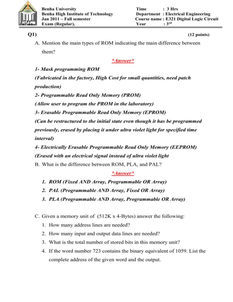
Benha University Benha High Institute of Technology Jan 2011 – Fall semester Exam (Regular), Q1) Time : 3 Hrs Department : Electrical Engineering Course name : E321 Digital Logic Circuit Year : 3rd Time Allowed: Hours (12 points) A. Mention the main types of ROM indicating the main difference between them? *Answer* 1- Mask programming ROM (Fabricated in the factory, High Cost for small quantities, need patch production) 2- Programmable Read Only Memory (PROM) (Allow user to program the PROM in the laboratory) 3- Erasable Programmable Read Only Memory (EPROM) (Can be restructured to the initial state even though it has be programmed previously, erased by placing it under ultra violet light for specified time interval) 4- Electrically Erasable Programmable Read Only Memory (EEPROM) (Erased with an electrical signal instead of ultra violet light B. What is the difference between ROM, PLA, and PAL? *Answer* 1. ROM (Fixed AND Array, Programmable OR Array) 2. PAL (Programmable AND Array, Fixed OR Array) 3. PLA (Programmable AND Array, Programmable OR Array) C. Given a memory unit of (512K x 4-Bytes) answer the following: 1. How many address lines are needed? 2. How many input and output data lines are needed? 3. What is the total number of stored bits in this memory unit? 4. If the word number 723 contains the binary equivalent of 1059. List the complete address of the given word and the output. *Answer* 1. Address lines = 19bit 2. Data Lines = 4bytes = 32 bit 3. Total Number of Bits = 512*1024*32 = 219*25 = 224 = 16777216 bit 4. Address = 1011010011 5. Data = 10000100011 Q2) (12 points) Utilizing necessary number of 512K x 8-bit RAM modules; construct the following: a. A 2M x 8-bit RAM module. b. A 512K x 32-bit RAM module. c. A 1M x 16-bit RAM module. *Answer* (Q2-A) (A 2M x 8-bit RAM) (Q2-B) (A 512K x 32-bit RAM) (Q2-C)(1MX16 ROM) Q3) Design a sequential circuit to perform the function of 4-bit BCD counter T- Flip-Flop. (8 points) using *Answer* A(t) B(t) C(t) D(t) A(t+1) B(t+1) C(t+1) D(t+1) TA TB TC TD 0 0 0 0 0 0 0 1 0 0 0 1 0 0 0 1 0 0 1 0 0 0 1 1 0 0 1 0 0 0 1 1 0 0 0 1 0 0 1 1 0 1 0 0 0 1 1 1 0 1 0 0 0 1 0 1 0 0 0 1 0 1 0 1 0 1 1 0 0 0 1 1 0 1 1 0 0 1 1 1 0 0 0 1 0 1 1 1 1 0 0 0 1 1 1 1 1 0 0 0 1 0 0 1 0 0 0 1 1 0 0 1 0 0 0 0 1 0 0 1 TC TB TA TB 0 1 1 0 0 0 1 0 0 0 0 0 0 1 1 0 0 0 1 0 0 0 1 0 X X X X X X X X X X X X 0 0 X X 0 0 X X 0 1 X X TD = 1 TC = A\D TB = CD TA = BCD + AD (Q3) Q4) (16 points) A. Design a combinational circuit using a ROM. The circuit accepts a 3-bit number (x; where x = x2x1x0) and generate an output binary number equal to the square of the input number plus the number plus one (x2 - x + 1). *Answer* I/P A B C O/P Q1 Q2 Q3 Q4 Q5 Q6 0 0 0 0 1 0 0 0 0 0 1 1 0 0 1 1 0 0 0 0 0 1 2 0 1 0 3 0 0 0 0 1 1 3 0 1 1 7 0 0 0 1 1 1 4 1 0 0 13 0 0 1 1 0 1 5 1 0 1 21 0 1 0 1 0 1 6 1 1 0 31 0 1 1 1 1 1 7 1 1 1 43 1 0 1 0 1 1 Q6 = Σ(0,1,2,3,4,5,6,7) = 1 Q5 = Σ(2,3,6,7) = B Q4 = Σ(3,4,5,6) = A B\ + AC\ + A\BC Q3 = Σ (4,6,7) = AB + AC\ Q2 = Σ (5,6) = AB\C + ABC\ Q1 = Σ (7) = ABC B. Design the same problem of Q4.A using PLA. Q5) (12 points) A. Writ e an appropriate VHDL code that describes a 2x4 active high decoder. Demonstrate your answer with a block indicating all the inputs and the outputs as well as a truth table of the required decoder. *Answer* Entity dec2x4 is Port (I: in std_logic_vector(1 downto 0); D: out std_logic_vector(3 downto 0)); End dec2x4; Architecture arch1 of dec2x4 is Begin With I select D <= "1000" when "00", "0100" when "01", "0010" when "10", "0001" when "11", "0000" when others; End arch1; B. Write a concurrent VHDL code to represent the below logic circuit. *Answer* ENTITY example2 IS PORT (xl, x2, x3, x4: IN BIT; f, g : OUT BIT); END example2 ; ARCHITECTURE LogicFunc OF example2 IS BEGIN f <= (xl AND x3) OR (NOT x3 AND x2); g <= (NOT x3 OR xl) AND (NOT x3 OR x4) ; END LogicFunc
