High-efficiency Nanowire Array Solar Cells by Radioisotope
advertisement
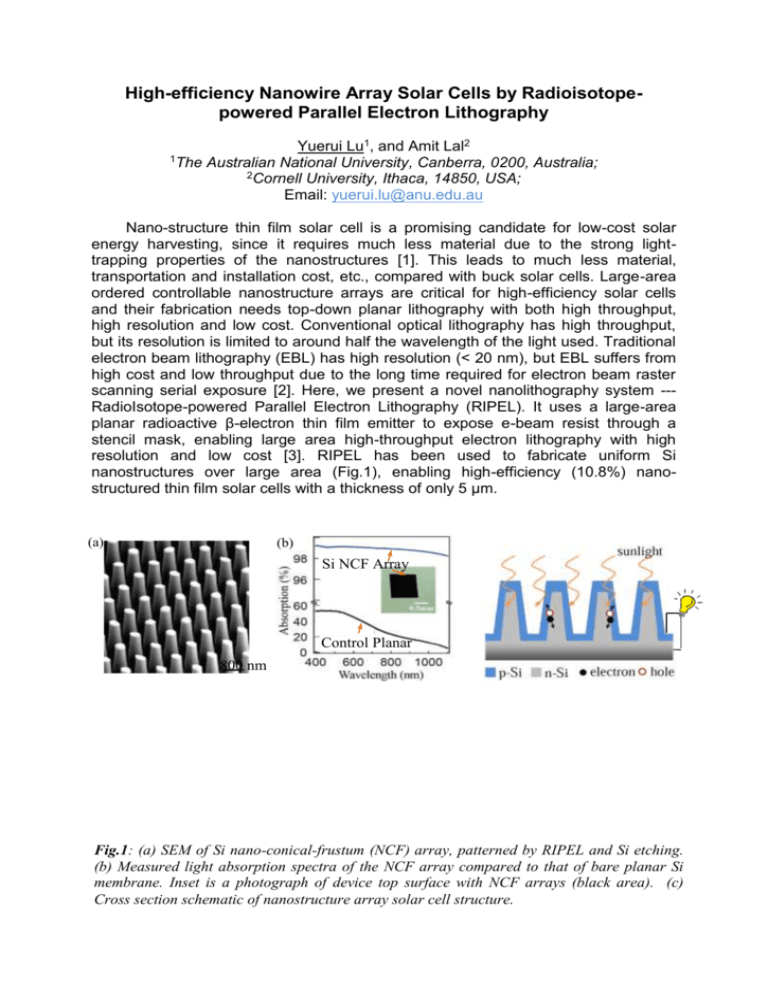
High-efficiency Nanowire Array Solar Cells by Radioisotopepowered Parallel Electron Lithography Yuerui Lu1, and Amit Lal2 1The Australian National University, Canberra, 0200, Australia; 2Cornell University, Ithaca, 14850, USA; Email: yuerui.lu@anu.edu.au Nano-structure thin film solar cell is a promising candidate for low-cost solar energy harvesting, since it requires much less material due to the strong lighttrapping properties of the nanostructures [1]. This leads to much less material, transportation and installation cost, etc., compared with buck solar cells. Large-area ordered controllable nanostructure arrays are critical for high-efficiency solar cells and their fabrication needs top-down planar lithography with both high throughput, high resolution and low cost. Conventional optical lithography has high throughput, but its resolution is limited to around half the wavelength of the light used. Traditional electron beam lithography (EBL) has high resolution (< 20 nm), but EBL suffers from high cost and low throughput due to the long time required for electron beam raster scanning serial exposure [2]. Here, we present a novel nanolithography system --RadioIsotope-powered Parallel Electron Lithography (RIPEL). It uses a large-area planar radioactive β-electron thin film emitter to expose e-beam resist through a stencil mask, enabling large area high-throughput electron lithography with high resolution and low cost [3]. RIPEL has been used to fabricate uniform Si nanostructures over large area (Fig.1), enabling high-efficiency (10.8%) nanostructured thin film solar cells with a thickness of only 5 μm. (a) (b) Si NCF Array 800 nm Control Planar Si Fig.1: (a) SEM of Si nano-conical-frustum (NCF) array, patterned by RIPEL and Si etching. (b) Measured light absorption spectra of the NCF array compared to that of bare planar Si membrane. Inset is a photograph of device top surface with NCF arrays (black area). (c) Cross section schematic of nanostructure array solar cell structure. References [1] [2] [3] Zhu, J., Hsu, C.-M., Yu, Z., Fan, S. & Cui, Y. Nanodome Solar Cells with Efficient Light Management and Self-Cleaning. Nano Letters 10, 1979-1984 (2009). C. Vieu) et al. Electron beam lithography: resolution limits and applications. Applied Surface Science 164, 111–117 (2000). Lu, Y. & Lal, A. Vacuum-Free Self-Powered Parallel Electron Lithography with Sub-35-nm Resolution. Nano Letters 10, 2197-2201 (2010).
