Electrical Transduction in Nanomechanical
advertisement
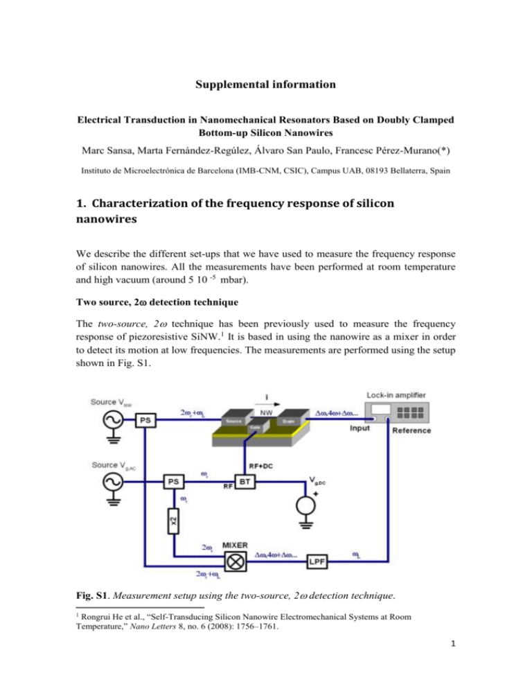
Supplemental information Electrical Transduction in Nanomechanical Resonators Based on Doubly Clamped Bottom-up Silicon Nanowires Marc Sansa, Marta Fernández-Regúlez, Álvaro San Paulo, Francesc Pérez-Murano(*) Instituto de Microelectrónica de Barcelona (IMB-CNM, CSIC), Campus UAB, 08193 Bellaterra, Spain 1. Characterization of the frequency response of silicon nanowires We describe the different set-ups that we have used to measure the frequency response of silicon nanowires. All the measurements have been performed at room temperature and high vacuum (around 5 10 -5 mbar). Two source, 2 detection technique The two-source, 2 technique has been previously used to measure the frequency response of piezoresistive SiNW.1 It is based in using the nanowire as a mixer in order to detect its motion at low frequencies. The measurements are performed using the setup shown in Fig. S1. Fig. S1. Measurement setup using the two-source, 2 detection technique. Rongrui He et al., “Self-Transducing Silicon Nanowire Electromechanical Systems at Room Temperature,” Nano Letters 8, no. 6 (2008): 1756–1761. 1 1 In this measurement technique, a voltage is applied to the nanowire with the form: 𝑉𝑁𝑊,2𝑠2𝑤 (𝑡) = 𝑉𝑁𝑊 𝑐𝑜𝑠((2𝜔𝑐 + 𝜔𝐿 )𝑡). (1) In order to actuate the nanowire, the following voltage is applied to the side-gate: 𝑉𝑔,2𝑠2𝑤 (𝑡) = 𝑉𝑔,𝐷𝐶 + 𝑉𝑔,𝐴𝐶 𝑐𝑜𝑠(𝜔𝑐 𝑡). (2) The deflection at the center of the nanowire x(t) caused by a sinusoidal excitation force (like that applied by the side-gate) takes the form: 𝑥(𝑡) = 𝑥0 (𝜔) cos(𝜔𝑡). (3) The nanowire has a resistance at rest R0. Its motion causes a certain elongation, which in turn provokes a change in its resistance due to the piezoresistive effect. This resistance change R is described for the first mode of resonance as:2 ∆𝑅 𝑥 2 (𝑡) = ̃ 2.44𝐺𝑃𝑅 2 . 𝑅0 𝐿 (4) Where GPR is the gauge factor and L is the length of the nanowire. If R<<R0 (in our case, R/R0 <10-3), then the expression for the current flowing through the nanowire can be approximated as: 𝑖𝑁𝑊 = 𝑉𝑁𝑊,2𝑠2𝑤 𝑉𝑁𝑊,2𝑠2𝑤 ∆𝑅 = ̃ (1 − ). 𝑅0 + ∆𝑅 𝑅0 𝑅0 (5) This expression contains two terms: the purely electrical term due to the resistance of the nanowire and a second term related to its motion. Discarding the purely electrical term, high-frequency and DC components (which take place at other frequencies, and therefore do not affect the measurements), the term at frequency L due to the motion of the nanowire is: 𝑉𝑁𝑊,2𝑠2𝑤 ∆𝑅 𝑅0 𝑅0 𝑉𝑁𝑊 𝑥02 (𝜔𝑐 ) = 2.44𝐺𝑃𝑅 𝑐𝑜𝑠 2 (𝜔𝑐 𝑡)𝑐𝑜𝑠((2𝜔𝑐 + 𝜔𝐿 )𝑡) 𝑅0 𝐿2 𝑖𝑁𝑊,𝑚𝑜𝑡𝑖𝑜𝑛𝑎𝑙 = − 𝑖𝑁𝑊,𝑚𝑜𝑡𝑖𝑜𝑛𝑎𝑙,𝜔𝐿 = 0.61 2 𝑉𝑁𝑊 𝐺𝑃𝑅 𝑥02 (𝜔𝑐 ) 𝑐𝑜𝑠(𝜔𝐿 𝑡). 𝑅0 𝐿2 (6) (7) Ibid. 2 Two source, 1 detection technique The two-source, 1 has been used to detect the motion of carbon nanotube (CNT) resonators, in which the transduction of their motion is due to the conductance modulation caused by a change in the capacitance between the nanowire and the sidegate. This technique is similar to the two-source, 1 but adapted to this transduction mechanism, in which the transduced signal is proportional to the motion of the nanowire. The measurements are performed using the setup of Fig. S2. Fig. S2. Measurement setup using the two-source, 1 detection technique. In this case the voltage applied to the nanowire is: 𝑉𝑁𝑊,2𝑠1𝑤 (𝑡) = 𝑉𝑁𝑊 𝑐𝑜𝑠((𝜔𝑐 + 𝜔𝐿 )𝑡). (8) Note that in this case the signal is at a frequency near c, unlike in the two-source, 2 technique. The gate voltage and the motion of the nanowire take the same form that with the two-source, 2 technique. If the transduction is caused by the conductance change due to the change in capacitance with the side-gate, the low frequency current (which is developed elsewhere3) takes the form: V. Sazonova et al., “A Tunable Carbon Nanotube Electromechanical Oscillator,” Nature 431, no. 7006 (September 2004): 284–287. 3 3 𝛿𝐼𝐿𝐼𝐴,2𝑠1𝑤 = 𝛿𝐶𝑔 1 𝑑𝐺 (𝑉𝑔,𝐴𝐶 + 𝑉𝑔,𝐷𝐶 ) 𝑉𝑁𝑊 . 𝐶𝑔 2√2 𝑑𝑉𝑔 (9) Where dG/dVg is the transconductance of the nanowire and Cg/Cg is the relative change of capacitance between the nanowire and the excitation side-gate due to its motion. An estimation of the transconductance dG/dVg can be found by evaluating the first term of the equation, which corresponds to the parasitic signal. Measuring the electrical background of the signal at a frequency c far away from resonance, the transconductance value is defined as: 𝛿𝐼𝐿𝐼𝐴,𝑏𝑎𝑐𝑘𝑔𝑟𝑜𝑢𝑛𝑑 𝑑𝐺 = 2√2 . 𝑑𝑉𝑔 𝑉𝑔,𝐴𝐶 𝑉𝑁𝑊 (10) 2. Measurements using the FM method In our work we have used the frequency modulation (FM) detection technique to characterize silicon nanowire (SiNW) resonators. With this method, the voltage applied to the nanowire is: 𝜔Δ (11) 𝑐𝑜𝑠(𝜔𝐿 𝑡)) 𝜔𝐿 Where c is the high-frequency carrier component, which also acts as the excitation frequency of the nanowire; L is the low frequency readout component and is the frequency deviation. Following the development described elsewhere,4 the transduction signal is proportional to the motion of the nanowire, and the low-frequency current detected by the lock-in amplifier can be expressed as: 𝑉𝑁𝑊,𝐹𝑀 (𝑡) = 𝑉𝑁𝑊 𝑐𝑜𝑠 (𝜔𝑐 𝑡 + 𝜕𝑅𝑒(𝑥(𝜔)) 1 𝜕 2 𝐼𝑁𝑊 (12) 𝐼𝜔𝐿,𝐿𝐼𝐴 = 𝑉𝑁𝑊 𝜔Δ cos(𝜔𝐿 𝑡) 2 𝜕𝑥𝜕𝑉𝑁𝑊 𝜕𝜔 Where x() is the response of the nanowire to an excitation force F=F0cos(t). The term 𝜕2INW/ 𝜕x𝜕VNW depends on the transduction mechanism. As described by the term 𝜕Re(x())/𝜕, the amplitude of IL,LIA with varying excitation frequency c follows the shape of the real part of the derivative of the frequency response of the resonator. The frequency response of the nanowire in linear regime is described by the equation: Vincent Gouttenoire et al., “Digital and FM Demodulation of a Doubly Clamped Single-Walled CarbonNanotube Oscillator: Towards a Nanotube Cell Phone,” Small 6, no. 9 (May 7, 2010): 1060–1065. 4 4 𝑥(𝜔) = 𝐹 1 𝑚𝑒𝑓𝑓 𝜔2 − 𝜔 2 + 𝑖 𝜔0 𝜔 0 𝑄 (13) We fit the experimental frequency response of a resonator to equation (12) (Fig. S3). We find a good agreement of the experimental results with the predicted response, and obtain a quality factor (Q) of 3200 for this device. This is in good agreement with previous measurements of similar devices at room temperature.5 Equation (12) shows that the measured current is proportional to the frequency deviation This relationship holds as long as the frequency deviation is much smaller than the width of the resonance peak, otherwise the experimental response widens with respect to the predicted one.6 This is important because in order to correctly measure the quality factor of the resonators the value of has to be sufficiently small, which also causes a diminution of the amplitude and therefore of the signal-to-noise ratio. In the main text, some of the figures show widened responses in order to increase the magnitude of the output signals. Another particularity of the FM method is that the quality factor Q can be obtained graphically from the frequency response: the bandwidth of the response of the resonator (which determines Q) is the difference between the two minima of the FM response.7 We confirm this by comparing the graphically obtained value from the fitting in Fig. S3. Experimental Fit 120 Magnitude (pA) 100 80 60 40 20 0 66,00 66,05 66,10 66,15 Frequency (MHz) Fig. S3. Fitting of the frequency response of the fundamental mode of a nanowire with a length of 3m and a diameter of 87-95nm. We find a resonance frequency of around 66 MHz and a quality factor of 3200. 5 X.L. Feng et al., «Quality Factors and Energy Losses of Single-Crystal Silicon Nanowire Electromechanical Resonators» (IEEE, 2007), 1325–1326, 6 Gouttenoire et al., “Digital and FM Demodulation of a Doubly Clamped Single-Walled CarbonNanotube Oscillator.” 7 A. Eichler et al., “Nonlinear Damping in Mechanical Resonators Made from Carbon Nanotubes and Graphene,” Nature Nanotechnology 6, no. 6 (May 15, 2011): 339–342. 5 3. Simulations In order to validate the measurements, a model of the system has been developed. This model is specifically designed to evaluate the spectral components of the transduced signal using different detection techniques and transduction principles. The simulations are performed using MathWorks Matlab and Simulink R2007. Fig. S4a shows a schematic of the simulation schematic for the FM transduction technique and 1 transduction. The schematic includes the actuation/detection setup and the response of the resonator, which is defined as a linear transference function based on the model of equation (13). Similar schematics have been built for each detection method and transduction scheme. From this schematic, and varying the FM carrier frequency c we can simulate a frequency sweep. Fig. S4b shows the result of one of such sweeps, obtained by plotting the amplitude of the low frequency signal at the output of the simulation while varying the excitation frequency c. This kind of sweeps can be used to evaluate the effectiveness of each detection technique for the different transduction mechanisms. Fig. S4c shows the detection results, in the case of assuming a pure 1 transduction, when using the two-source, 1 and two-source, 2 detection set-ups. We corroborate that for pure 1 transduction, the signal detected using the two-source, 1 detection method should be much higher (about 30 times) than with the two-source, 2technique. 6 Low frequency signal FM-modulated voltage through the nanowire Force applied to the resonator Current detected by the Lock-in amplifier Response of the resonator Resistance of the nanowire (transduced signal) RF Source Nanowire Detection (a) 3,5 0,050 Q=1000 Q=750 Q=500 0,045 Magnitude (a.u.) Magnitude (u.a.) 0,040 0,035 0,030 0,025 0,020 0,015 0,010 0,005 0,000 44,50 2 source, 1w 2 source, 2w 3,0 2,5 2,0 1,5 1,0 0,5 0,0 44,75 45,00 45,25 Frequency (MHz) (b) 45,50 9,7 9,8 9,9 10,0 10,1 10,2 10,3 Frequency (MHz) (c) Fig. S4. Simulink simulations. (a) Simulation schematic of the FM transduction method for a 1 transduction. (b) Frequency response for different quality factors obtained by the schematic. The response is obtained by monitoring the amplitude of the low frequency signal, as with the experimental setup. For this simulation, f0=45 MHz. (c) Frequency response for different detection methods (two-source, 1 and two-source, 2), and pure 1 transduction. For this simulation, f0=10 MHz. Another application of the simulations is monitoring the frequency response of the system. The different frequency components generated by the setup can be found by simulating the system with fixed parameters at stationary regime. Fig. 4 in the main text shows an example of this kind of simulations for a nanowire in resonance, for different detection techniques and transduction mechanisms. This allows evaluating the efficiency of each of the different detection schemes for each transduction principle. 7 4. Static and dynamic motion of the nanowire For electrostatic actuation, the nanowire is excited into motion by means of a voltage applied to an electrode placed near the resonator. This voltage is composed by a DC voltage Vg,DC and an AC component Vg,AC, where typically Vg,DC>> Vg,AC in order to avoid quadratic terms in the excitation. Under these conditions, the force applied to the resonator is: 1 𝑑𝐶𝑔 𝐹𝑁𝑊 = 2 𝑑𝑥 1 𝑑𝐶𝑔 𝑉𝑔2 = ̃2 𝑑𝑥 𝑉𝑔,𝐷𝐶 (𝑉𝑔,𝐷𝐶 + 2𝑉𝑔,𝐴𝐶 ). (14) Where dCg/dx is the derivative of the capacitance between the nanowire and the side gate as a function of the displacement of the nanowire x. This expression has two different terms: the first one represents a DC static term and the second one an AC component at the excitation frequency. As a first approximation the response of the nanowire to an applied force can be described using the mass-spring model, following F=xk. Here, x is the motion of the resonator and k its elastic constant. Combining these expressions, the static deflection of the nanowire is: 𝐹𝑁𝑊,𝐷𝐶 = 2 𝑑𝐶𝑔 𝑉𝑔,𝐷𝐶 1 𝑑𝐶𝑔 2 𝑉𝑔 = 𝑘𝑥 → 𝑥𝑁𝑊,𝑠𝑡𝑎𝑡𝑖𝑐 = . 2 𝑑𝑥 𝑑𝑥 2𝑘 (15) The same method can be used for the dynamic motion. As we are interested in the motion in resonance, here the expression also includes the quality factor of the resonator: 𝐹𝑁𝑊,𝐴𝐶 = 𝑑𝐶𝑔 𝑑𝑥 𝑉𝑔,𝐴𝐶 𝑉𝑔,𝐷𝐶 , 𝑥𝑁𝑊,𝑟𝑒𝑠𝑜𝑛𝑎𝑛𝑐𝑒 = 𝐹𝑁𝑊,𝐴𝐶 𝑄 . 𝑘 (16) (17) Then the relationship between both amplitudes is: 𝑥𝑁𝑊,𝑟𝑒𝑠𝑜𝑛𝑎𝑛𝑐𝑒 𝑥𝑁𝑊,𝑠𝑡𝑎𝑡𝑖𝑐 𝑉𝑔,𝐴𝐶 = 2𝑄 𝑉 𝑔,𝐷𝐶 . (18) 8 5. Fabrication SiNW are directly grown in pre-patterned silicon chips by means of the vapor-liquidsolid mechanism.8 This process allows to obtain epitaxial contacts of the nanowires with the side-walls of microfabricated silicon trenches9 providing high quality electric contacts and an almost perfect clamping. The nanowires are grown in micro-trenches connecting two electrodes, with a silicon post acting as a side-gate electrode placed in very close proximity, which is used to actuate the nanowires electrostatically. We have used silicon-on-insulator (SOI) wafers as a substrate, with a highly doped silicon device layer, 2+/-0.5 m thick and <110> orientation. A 0.5 m buried oxide electrically insulates the top silicon layer from the bulk silicon. The contact electrodes, trenches and side-gate are patterned in the device layer using optical photolithography and reactive ion etching. After that, Au catalyst particles are randomly deposited on the substrate from a colloidal solution (BBInternational, diameter of 50nm). Then, the silicon nanowires are grown in a home-made atmospheric pressure CVD at 800ºC using SiCl4 as a precursor and Ar/H2 10% as carrier gas, following a process described elsewhere.10 The nanowires grow from the gold catalyst particles with a diameter determined by their size, following the <111> direction of the Si substrate. Finally, the nanowires are doped ex-situ, by annealing the chips for 1 hour at temperatures from 850-1000ºC in close proximity to a boron nitride wafer. It is important to note that although the deposition process of the catalyst is random, by controlling the colloid density and the trench width we can obtain nanowires placed in close proximity to the side-gate. Using this method we obtain a fabrication yield in the order of 5% of functional resonators, which is enough to obtain several devices per chip due to the parallel nature of the whole fabrication process. R. S. Wagner and W. C. Ellis, “VAPOR-LIQUID-SOLID MECHANISM OF SINGLE CRYSTAL GROWTH,” Applied Physics Letters 4, no. 5 (1964): 89. 9 Anurag Chaudhry et al., “Ultra-low Contact Resistance of Epitaxially Interfaced Bridged Silicon Nanowires,” Nano Letters 7, no. 6 (June 2007): 1536–1541. 10 Álvaro San Paulo et al., “Suspended Mechanical Structures Based on Elastic Silicon Nanowire Arrays,” Nano Letters 7, no. 4 (April 2007): 1100–1104. 8 9
