Supplementary material: The initial materials for the accumulative
advertisement
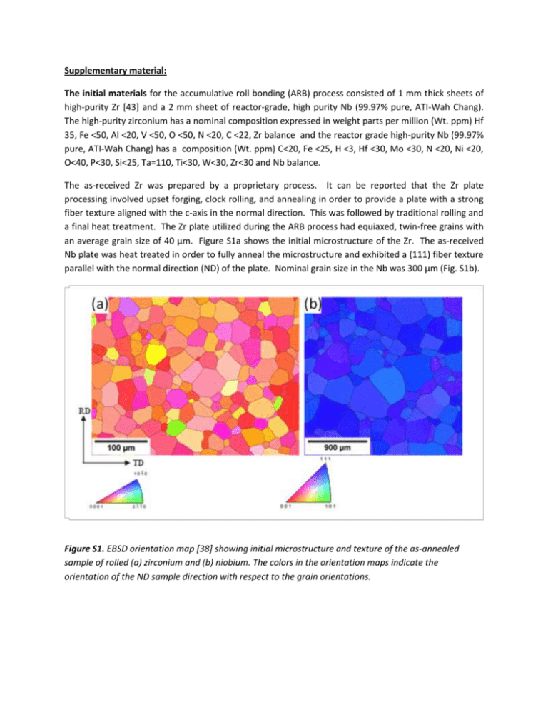
Supplementary material: The initial materials for the accumulative roll bonding (ARB) process consisted of 1 mm thick sheets of high-purity Zr [43] and a 2 mm sheet of reactor-grade, high purity Nb (99.97% pure, ATI-Wah Chang). The high-purity zirconium has a nominal composition expressed in weight parts per million (Wt. ppm) Hf 35, Fe <50, Al <20, V <50, O <50, N <20, C <22, Zr balance and the reactor grade high-purity Nb (99.97% pure, ATI-Wah Chang) has a composition (Wt. ppm) C<20, Fe <25, H <3, Hf <30, Mo <30, N <20, Ni <20, O<40, P<30, Si<25, Ta=110, Ti<30, W<30, Zr<30 and Nb balance. The as-received Zr was prepared by a proprietary process. It can be reported that the Zr plate processing involved upset forging, clock rolling, and annealing in order to provide a plate with a strong fiber texture aligned with the c-axis in the normal direction. This was followed by traditional rolling and a final heat treatment. The Zr plate utilized during the ARB process had equiaxed, twin-free grains with an average grain size of 40 μm. Figure S1a shows the initial microstructure of the Zr. The as-received Nb plate was heat treated in order to fully anneal the microstructure and exhibited a (111) fiber texture parallel with the normal direction (ND) of the plate. Nominal grain size in the Nb was 300 μm (Fig. S1b). Figure S1. EBSD orientation map [38] showing initial microstructure and texture of the as-annealed sample of rolled (a) zirconium and (b) niobium. The colors in the orientation maps indicate the orientation of the ND sample direction with respect to the grain orientations. The ARB process involves stacking plates of material and then performing a rolling operation on the stack such that a large enough reduction occurs during a single pass to induce bonding between the initially separate sheets. The Zr and Nb plates, after initial processing, were cleaned in an ultrasonic acetone bath and then wire brushed. This surface preparation was repeated prior to all ARB steps. Zr was placed on both the top and bottom of the Nb plate, similar to the copper-cladding technique described in [22], to build the initial stack. The stack was then rolled to a 50% reduction via a single highstrain rolling pass on a 2-high rolling mill (Waterbury-Farrel). After successful roll bonding, the plate was cut in half and stacked such that the process could be repeated. In this way, material was fabricated that had various nominal layer thicknesses and various amounts of accumulated strain. In this study, intermediate annealing treatments were utilized in order to mitigate the effect of shear banding. Anneals at 575°C for 60 minutes were performed after every second roll bonding pass or at strain intervals of 1.4. The time and temperature combination was chosen in order to minimize large amounts of intermixing of the Zr and Nb which occurs above temperatures of ~500°C [50]. Characterization was performed after both roll bonding steps and annealing treatments. Table S1 provides the layer thicknesses and total strain (see Eqn 1) associated with each sample that was investigated in this study. Table S1. Number of layers, layer thickness, total strain and latest processing step for the material characterized through neutron diffraction. A (*) indicates samples that have corresponding EBSD data. Total Strain, 𝜺 Latest Processing Step 2 Average Layer Thickness, h, μm 845 0.9 Roll Bonding 4 466* 1.5 Roll Bonding 4 466* 1.5 Annealing 8 198 2.3 Roll Bonding 16 106 2.9 Roll Bonding 16 106* 2.9 Annealing 32 59* 3.5 Roll Bonding 64 26 4.3 Roll Bonding 64 26 4.3 Annealing 128 12 5.1 Roll Bonding 256 6 5.8 Roll Bonding Number of Layers 256 6 5.8 Annealing 512 3 6.5 Roll Bonding 1024 1.5* 7.2 Roll Bonding 1024 1.5* 7.2 Annealing 2048 0.676 8.0 Roll Bonding 16384 0.092 10.0 Roll Bonding It should be noted that further roll bonding steps and annealing treatments were performed in between h = 676 nm and h = 92 nm. Material was not removed for characterization in those intervening steps in order to conserve the remaining material so that a goal of h < 100 nm could be reached. The sample of h = 92 nm represented two roll bonding steps since the previous heat treatment when the number of layers = 4096. Neutron diffraction (NeD) was performed on both the initial materials and processed samples using the High Pressure Preferred Orientation (HIPPO) neutron time-of-flight diffractometer at the Los Alamos Neutron Science Center at Los Alamos National Laboratory [54, 55]. Neutron diffraction provides a bulk measurement of specimen texture. The techniques used for both the collection of NeD data and the accompanying analysis to capture phase-specific orientation distribution functions (ODFs) was consistent with those described for the Cu-Nb system [21]. A small change within the HIPPO diffractometer set-up is the addition of two new detector panels at 2θ = 60° and 120°. Transmission electron microscopy (TEM) was used in order to investigate the planarity of the interfaces, confirm the nominal thickness (h) of the layers, and perform EDS line profile analysis for h = 92 nm. Bright Field TEM and chemical analysis was performed using a Tecnai F30 (FEI, Hillsboro, OR, USA) electron microscope operating at 300 kV on cross-sectional samples viewed along the TD. The samples were prepared using a traditional method of tripod polishing, dimpling, and ion milling. Electron back scatter diffraction (EBSD) on a scanning electron microscope (SEM) was performed at LANL on an FEI XL30 and an FEI InspectF SEM (FEI, Hillsboro, OR, USA) using the TSL/EDAX EBSD camera and software (TSL, Draper, UT, USA). Samples were prepared for EBSD by cross-sectioning, mounting, grinding and polishing with the final two polishing steps consisting of vibratory polishing using MasterPrep (Buehler) on a MasterTex cloth (Buehler) for four hours and Colloidal Silica (Allied) on a MasterTex cloth (Buehler) for fifteen minutes. The mounting method chosen was a low temperature epoxy mount in order to prevent the temperature associated with hot mounting from affecting grain morphology. In order to obtain good EBSD patterns from Zr layers, it was necessary to chemically polish the surface with a solution of the ratio 45H2O:45HNO3:10HF. EBSD was performed on the samples labeled with an * in Table S1. The EBSD scans were used to obtain texture information, grain morphology, and layer morphology. Steps sizes of 0.50 μm were used with areas scanned of 5000 μm2 for h>1.5 μm and steps sizes of 0.20 μm with areas scanned of 20000 μm2 for h = 1.5 μm.
