Diffuse scattering in scanning x-ray nanodiffraction
advertisement

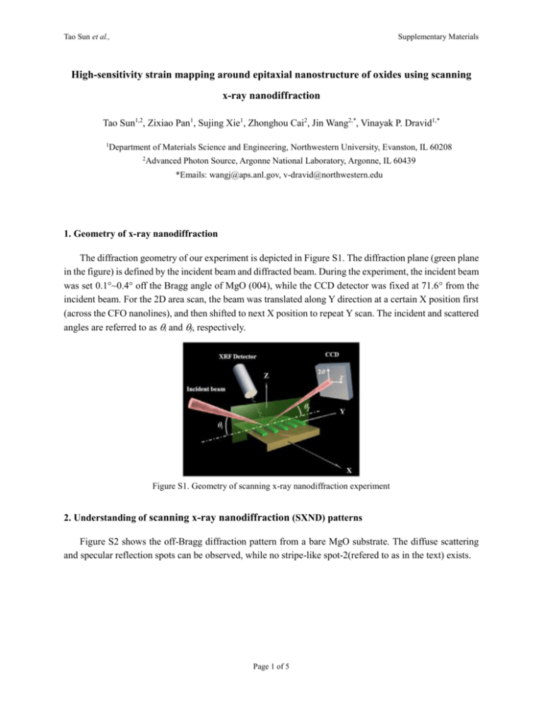
Tao Sun et al., Supplementary Materials High-sensitivity strain mapping around epitaxial nanostructure of oxides using scanning x-ray nanodiffraction Tao Sun1,2, Zixiao Pan1, Sujing Xie1, Zhonghou Cai2, Jin Wang2,*, Vinayak P. Dravid1,* 1 Department of Materials Science and Engineering, Northwestern University, Evanston, IL 60208 2 Advanced Photon Source, Argonne National Laboratory, Argonne, IL 60439 *Emails: wangj@aps.anl.gov, v-dravid@northwestern.edu 1. Geometry of x-ray nanodiffraction The diffraction geometry of our experiment is depicted in Figure S1. The diffraction plane (green plane in the figure) is defined by the incident beam and diffracted beam. During the experiment, the incident beam was set 0.1~0.4 off the Bragg angle of MgO (004), while the CCD detector was fixed at 71.6 from the incident beam. For the 2D area scan, the beam was translated along Y direction at a certain X position first (across the CFO nanolines), and then shifted to next X position to repeat Y scan. The incident and scattered angles are referred to as i and f, respectively. Figure S1. Geometry of scanning x-ray nanodiffraction experiment 2. Understanding of scanning x-ray nanodiffraction (SXND) patterns Figure S2 shows the off-Bragg diffraction pattern from a bare MgO substrate. The diffuse scattering and specular reflection spots can be observed, while no stripe-like spot-2(refered to as in the text) exists. Page 1 of 5 Tao Sun et al., Supplementary Materials Figure S2. Typical off-Bragg diffraction pattern from a bare MgO substrate 3. Result of m-factor fitting from another CoFe2O4 (CFO) nanoline Figure S3 shows the result of the fitted m-factor from the measurement of another CFO nanoline. Three characteristic peaks, two at the edges of the wetting layer and one at the central CFO nanoline, can be readily observed, which is consistent with the result shown in Figure 2(d) in the main text. Figure S3. Fitted m factor as a function of beam position. Three peaks correspond to two edges of the wetting layer and the central position of the CFO nanoline 4. Strain calculation (1) Edge-force model Page 2 of 5 Tao Sun et al., Supplementary Materials Assuming (1) a planar stress condition and (2) the length of CFO nanoline is much longer than its width, a simple edge-force model can be used. The stress components in the MgO substrate induced by a uniform CFO nanoline are given by 2 f tCFO ( y wCFO ) 3 y3 ( 2 ) yy 2 2 (y z ) (( y wCFO ) 2 z 2 ) 2 2 f tCFO 2 ( y wCFO ) y z ( 2 ) zz 2 2 ( y z ) (( y wCFO ) 2 z 2 ) 2 2 f tCFO ( y wCFO ) 2 y2 z ( 2 ) yz 2 2 (y z ) (( y wCFO ) 2 z 2 ) 2 (1) where y is the horizontal position coordinate with origin at one edge of CFO (note that the origin of the Y axes in all the figures is the starting point of scanning), and z is the depth coordinate with origin at the CFO/MgO interface; yy/zz and yz are the normal and shear stresses; f is the edge force; tCFO and wCFO are the thickness and width of the CFO nanoline (or wetting layer), respectively. f is the eigen-stress in CFO, which can be calculated as f e ECFO (1 CFO ) (2) where e is the eigen-strain in the system, which is the mismatch strain between CFO and MgO; ECFO and CFO denote the Young’s modulus and Poisson’s ratio of CFO, respectively. (2) Strain in the MgO substrate Since both CFO and MgO are cubic structure, the in-plane shear strain in MgO can be expressed as MgO 2 xyMgO s44 xx 2(s11 s12 ) xx 2(1 MgO ) / EMgO xx (3) For the CFO nanolines in our samples, there are four edges: two edges of central CFO line and two of the diffusion layer. In our model, the whole CFO nanoline is treated as two separate units: top central pattern and bottom diffusion layer, and all the edges are assumed to be sharp with side walls perpendicular to the substrate surface. Hence, the CFO-induced strain distribution in MgO substrate can be calculated as the superimposing of four edge forces, namely, two forces from the edges of the diffusion layer and another two forces from the edges of the central CFO pattern. By combining equations (1)-(3), the shear strain in the MgO substrate could be expressed as MgO ( y, z ) 4e1 tCFO,1 4e2 tCFO, 2 ECFO (1 MgO ) EMgO (1 CFO ) ( ( y12 y13 ( y1 w1 )3 ) 2 2 z ) (( y1 w1 ) 2 z 2 ) 2 (4) (1 CFO ) ( y2 w2 ) ( ) (1 CFO ) ( y22 ( z tCFO,1 ) 2 ) 2 (( y2 w2 ) 2 ( z tCFO,1 ) 2 ) 2 y23 3 where footnotes 1 and 2 denote components of the diffusion layer and the central CFO pattern, respectively; e1 is the eigen-strain at the interface of the CFO diffusion layer and the MgO substrate; e2 is the eigen-strain at the interface of the CFO central pattern and the diffusion layer. Page 3 of 5 Tao Sun et al., Supplementary Materials (3) Strain in the CFO diffusion layer and the top CFO nanoline In addition, it is also necessary to calculate the strain distribution within the CFO nanoline (both the top central pattern and the diffusion layer), as it also contributes to the diffuse scattering intensity. As the thickness of the diffusion layer is as thin as 2~3 nm, the strain variation along the out-of-plane direction can be negligible. Since the diffusion layer is sandwiched between the top CFO pattern and the bottom substrate, there are two types of stress exerted onto it: tensile stress by the MgO substrate and compressive stress by the top CFO nanoline. The strain distribution within the CFO diffusion layer is then considered as the combination of two strain fields. For the top CFO nanoline, the situation is simpler as it has only one interface with the diffusion layer. The strain in both of the CFO structures can be calculated with equations similar to those shown above. 5. Cross-section transmission electron microscopy (TEM) images Figure S4(a) shows annular dark field images (by JEM-2100F FEG FasTEM) of the cross section of a CFO nanoline with a nominal line width of 100 nm. It is clearly revealed that a few-nanometers-thickness wetting layer formed after high-temperature long-time thermal annealing. The TEM sample was fabricated using focused ion beam (FIB). Before FIB cutting, a thin layer of Pd/Au was sputtered on the sample onto make the surface conducting, and another two layers of amorphous Pt was deposited through a nozzle in the FIB to protect the surface of the sample from being damaged by Ga ion bombardment. A CFO nanoline, narrower than those studied in SXND experiments, was selected to compromise the field of view of TEM under appropriate magnification. Figure S4(b) and 4(c) show the high-resolution TEM (HRTEM) images of interface regions around the edge of the wetting layer and the edge of the central nanoline. The surface and interface of the CFO/MgO sample are indicated using red dashed lines in the images. Dislocations and other types of defects are indicated by yellow solid lines and arrows. Qualitatively, there are more defects at the regions around the edges in both MgO and CFO than at the center position of the CFO line (Figure 1(e) in the main text). Given that the primary driving force for forming defects is to release the elastic mismatch strain in the system, the larger degree of lattice imperfection is clear evidence for a more concentrated original strain field. However, quantitative TEM analysis will be difficult and lack of reliability as TEM sample preparation process could easily introduce structural defects. Page 4 of 5 Tao Sun et al., Supplementary Materials Figure S4. (a) Cross-section dark-field TEM image of a CFO nanoline; HRTEM images of CFO/MgO interface at (b) edge of the wetting layer, (c) edge of the central CFO line. The morphology of the CFO nanoline is outlined with red dashed lines, and the defects are indicated by yellow lines and arrows. Page 5 of 5


