The Analog-to-Digital Conversion Process: A Technical Description
advertisement
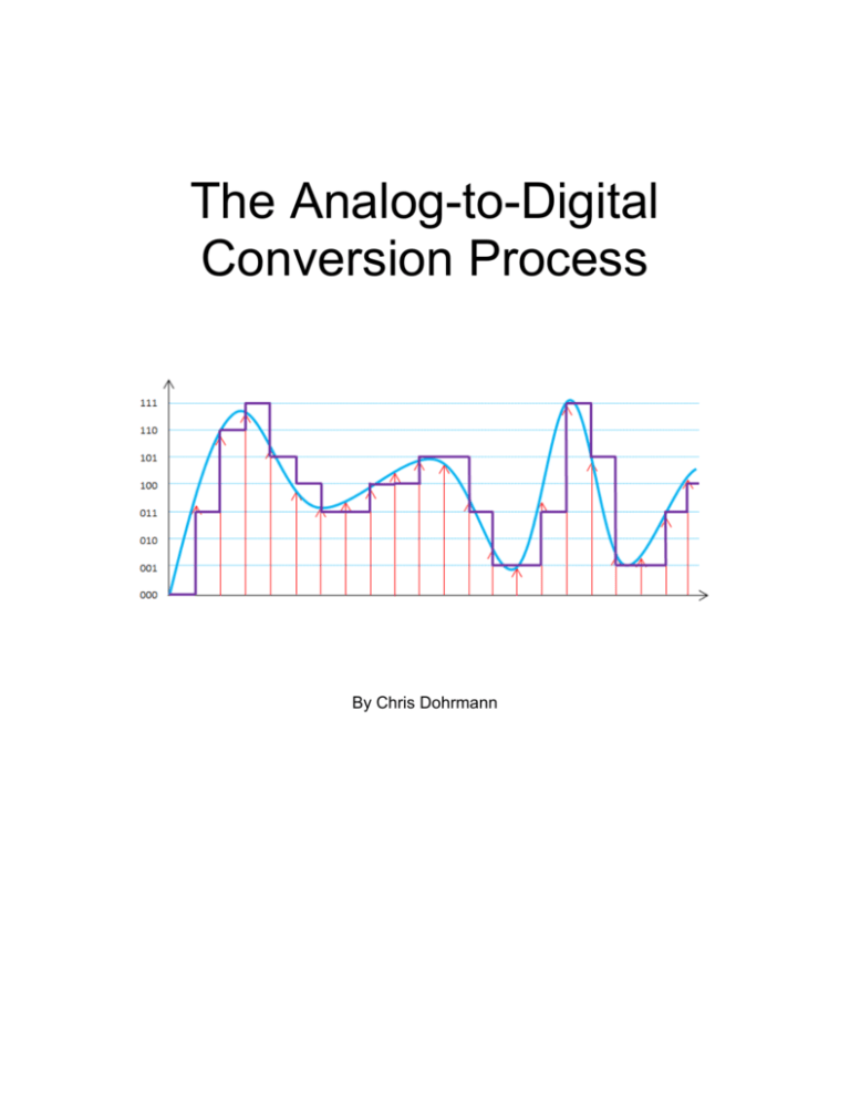
The Analog-to-Digital Conversion Process By Chris Dohrmann ADVANCE ORGANIZER ABOUT THIS DOCUMENT The purpose of this document is to provide readers with a technical description of the analog-to-digital conversion process performed by analog-to-digital converters (ADC’s). The scope of this document will include an overview of the process along with fundamental concepts and theory of operation. It will not include specifics about a particular method of analog-to-digital conversion, information about device physics or hardware design. ABOUT THE AUDIENCE Due to the technical nature of this document, readers should have a basic understanding of the following subjects: ˗ ˗ ˗ ˗ Analog and digital signals Sinusoids Complex exponentials Binary numbers After reading this document, the audience will have a general understanding of the fundamentals of the ADC process. This knowledge will be useful to readers who are interested in digital signal processing, embedded development, audio engineering, communications, or similar disciplines. With some basic knowledge of embedded development and digital design, in addition to the information in this document, it is possible to implement simple analog-to-digital conversion systems. 2 INTRODUCTION An analog-to-digital converter (ADC) is an electronic device that converts analog signals into digital representations. ADC’s can be found within almost all personal computers and smartphones. ADC’s are also used in commercial applications such as scientific measurement, digital signal processing, and audio recording. The process of analog-to-digital conversion can be broken down into three components; analog input, sampling, and digital output. INPUT OUTPUT ADC Figure 1 - Electrical symbol for an ADC Figure 2 – 8-channel 10-bit ADC (~$3.00) Figure 3 – 2GSPS 10-bit ADC (~$37,500) 3 THE PROCESS INPUT Voltage The most common analog input is voltage and because this is the only form of analog input that an ADC is capable of processing directly, it will be the focus of this document. To input a signal representing something such as sound, light, or force, a transducer (a device that converts energy into another form of energy) will be used. This transducer will take the original signal and transform it into an analog voltage signal with varying frequency and amplitude. Nearly all waveforms can be represented through a summation of various sinusoidal signals. An example of a time varying analog voltage input is shown below. Time Figure 4 – Time-varying analog voltage Common expressions of sinusoidal signals: 𝑓(𝑡) = 𝐴𝑐𝑜𝑠(𝜔𝑡 + 𝜃) (Sinusoidal) 𝐹 = 𝐴𝑒 𝑗𝜃 (Phasor) where 𝜔 = frequency and 𝑗 is the imaginary unit 4 SAMPLING Voltage While the analog signal is being fed through the input terminal the ADC will take voltage measurements at a predefined frequency. This process is known as sampling. The frequency of sampling (𝑓𝑠 ) is the rate at which samples are taken. 𝑓𝑠 is measured in hertz, so if you take 1000 samples per second 𝑓𝑠 = 1000Hz. This is the process responsible for transforming continuous time signals (analog) into discrete time signals (digital). By sampling an analog signal at the correct frequency it is possible to retain all or nearly all of the information contained in that signal in a digital form. Shown below is the result of sampling the original signal from the previous example. The arrows represent the measurements taken by the ADC. Time Figure 5 – Sampled time-varying analog voltage In order to be able to reproduce a sampled signal, it must be sampled at more than twice the highest frequency contained within that signal. 𝑓𝑠 ≥ 2𝐵 where 𝑓𝑠 is the frequency of sampling and 𝐵 is the highest frequency. (For a given band-limited signal) from Shannon-Nyquist sampling theorem A signal that is band-limited means that it contains a finite amount of frequencies Although taking these samples has transformed the original continuous time signal into a discrete time signal it still cannot be used by modern electronics. In order for this to be possible, these samples must be represented in binary code. 5 DIGITAL OUTPUT The process through which these samples are converted into binary code is called encoding. By equating voltage levels to binary numbers it is possible to write signals as a stream of binary numbers. Shown below is the result of applying this process to these samples. The horizontal dotted lines represent the levels that are associated with the binary values to the left. In this example the ADC has a resolution of 3. This means that there are 23 or 8 intervals that are recognized by the ADC. Higher resolution ADCs are available. 𝑇𝑜𝑡𝑎𝑙 𝑖𝑛𝑡𝑒𝑟𝑣𝑎𝑙𝑠 = 2𝑛 , 𝑤ℎ𝑒𝑟𝑒 𝑛 = 𝑟𝑒𝑠𝑜𝑙𝑢𝑡𝑖𝑜𝑛 (𝑖𝑛 𝑏𝑖𝑡𝑠) 111 110 101 100 011 010 001 000 Time Figure 6 – Assigning binary values to reference intervals 6 As shown by the picture on the previous page, some of these values fall between the specified levels. If this is the case, the value will be quantized, or rounded to the nearest level. Shown below is the result. Figure 7 – Quantizing sample values to reference levels So, instead of having a stream of values such as (0, 3, 6, 7 …) You will have a stream of bits (000011110111…) SOURCES OF ERROR There are a few sources of error that can be introduced through the analog-todigital conversion process. Quantization can introduce noise caused by rounding analog values to the nearest voltage levels. This is known as quantization error. Physical imperfections in the device may also cause error. Non-ideal clock properties are another common source of error DESIRABLE ADC SPECIFICATIONS & PRICING Today, simple ADC’s are available for less than $1.00, while those intended for commercial use can cost around $1000 (with more advanced ADC’s reaching prices as high as $35,000 or more). The difference in price is related to technical specifications such as sampling rate, resolution, and power usage. Some applications can require a sampling rate as high as 3+ Gigahertz or a resolution as high as 24+ bits. Lower power consumption is also a highly desirable trait. 7 Time CONCLUSION Analog-to-digital conversion is a powerful yet fundamentally simple process. By assigning binary values to voltage reference levels it is possible to convert analog signals into digital signals. Once this data has been converted into a digital form it can be passed through additional circuitry to perform additional functions or undergo further processing. This is what makes analog-to-digital conversion so important in modern technology. WORKS CITED Lathi, B.P. (1998). Modern Digital and Analog Communication Systems (3rd edition). Oxford University Press. "Digitization of Analog Quantities". Iamechatronics.com. Retrieved 2014-24-3. Figures 1 and 4-7 were created by Chris Dohrmann using Microsoft Word. Figures 2 & 3 were taken from www.adafruit.com and www.mouser.com respectively. 8
