Quantum Mechanical Compact Modeling of Inversion
advertisement
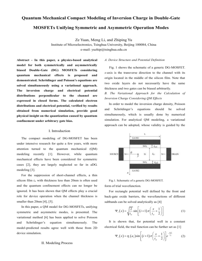
Quantum Mechanical Compact Modeling of Inversion Charge in Double-Gate MOSFETs Unifying Symmetric and Asymmetric Operation Modes Ze Yuan, Meng Li, and Zhiping Yu Institute of Microelectronics, Tsinghua University, Beijing 100084, China e-mail: yuzhip@tsinghua.edu.cn Abstract - In this paper, a physics-based analytical model for both symmetrically and asymmetrically biased Double-Gate quantum (DG) MOSFETs considering mechanical effects is proposed and demonstrated. Schrödinger and Poisson’s equations are solved simultaneously using a variational approach. The inversion distributions charge and perpendicular to electrical the potential channel are expressed in closed forms. The calculated electron distributions and electrical potential, verified by results obtained from numerical simulation, provide good A. Device Structure and Potential Definition Fig. 1 shows the schematic of a generic DG-MOSFET. x-axis is the transverse direction to the channel with its origin located in the middle of the silicon film. Note that two oxide layers do not necessarily have the same thickness and two gates can be biased arbitrarily. B. The Variational Approach for the Calculation of Inversion Charge Considering QM Effects In order to model the inversion charge density, Poisson and Schrödinger’s equations should be solved physical insight on the quantization caused by quantum simultaneously, which is usually done by numerical confinement under arbitrary gate bias. simulation. For analytical QM modeling, a variational approach can be adopted, whose validity is guided by the I. Introduction The compact modeling of DG-MOSFET has been under intensive research for quite a few years, with more attention turned to the quantum mechanical (QM) modeling recently [1]. However, while quantum mechanical effects have been considered for symmetric cases [2], they are largely neglected so far in aDG. modeling [3]. For the suppression of short-channel effects, a thin silicon film tsi with thickness less than 20nm is often used and the quantum confinement effects can no longer be Fig.1. Schematic of a generic DG-MOSFET. form of trial wavefunction. ignored. It has been shown that QM effects play a crucial For rectangle potential well defined by the front and role for device operation when the channel thickness is back-gate oxide barriers, the wavefunctions of different smaller than 20nm [4], [5]. subbands can be solved analytically as [4] In this paper, a QM model for DG-MOSFETs, unifying symmetric and asymmetric modes, is presented. The i x x 1 2 sin i 1 tsi tsi 2 (1) variational method [6] has been applied to solve Poisson and Schrödinger’s equation simultaneously. The model-predicted results agree well with those from 2D device simulation. II. Modeling Process It is shown that, for potential well in a constant electrical field, the trail function can be further set as [1] x 1 i i x i ai sin i 1 e tsi tsi 2 ax (2) where ai are undetermined parameter related to the boundary conditions, degree of asymmetry, and i ai are normalization constants. At zeros field, ai ox 0 , the wavefunctions are Vg1 V fb S1 tox1 si d dx (5) x tsi 2 identical to Eq. (1). In order to unify symmetric and asymmetric conditions, ox both the position of the peak of the electron distribution and the degree of asymmetry must be taken into considerations. Hence, we introduce three parameters ai , bi and ci to describe the generalized trial wavefunctions x 1 ax b x i x i sin i 1 ci exp i exp i tsi 2 tsi tsi (3) where i=0, 1, 2,…, and i ai , bi , ci is normalization coefficient so that tsi 2 t si 2 tox 2 si d dx (6) x tsi 2 the potential x can be obtained in closed form. The effectiveness of this approximation has been proven in [2]. IV. Summary A compact model unifying symmetric and asymmetric DG-MOSFET considering quantum confinement in transverse direction is presented. The variational approach is used to calculate energy level and wavefunction. 1D Schrödinger i 2 x dx 1 . Vg 2 V fb S 2 and Poisson’s equation are solved simultaneously. Comparison between the model predicted data and the numerical device simulation data further For symmetric biased conditions, ci 1 and the trail validates the accuracy of our model. wavefunctions are identical to Eq. (3). For extreme asymmetric cases, ai bi , hence have the same form as Eq. (2). Furthermore, it guarantees a smooth transition References [1] on the Threshold Voltage of Undoped Double-Gate between the two extreme cases. MOSFETs,” IEEE Electron Device Letters, vol. 26, no. 8, By employing the gradual channel approximation pp. 579-582, Aug. 2005. (GCA), the 1D Poisson’s equation in the direction [2] perpendicular to the channel has the general form of d 2 x dx 2 V. Trivedi, and J. Fossum, “Quantum-Mechanical Effects L. Ge, and J. Fossum, “Analytical Modeling of Quantization and Volume Inversion in Thin Si-Film DG q q N 2 x N A (4) n x N A si si inv where x is the electrostatic potential, n( x) is the MOSFETs,” IEEE Trans. Electron Devices, vol. 49, no. 2, pp. 287-294, Feb. 2002. [3] Symmetric and Asymmetric DG MOSFETs,” IEEE Trans. electron volume density, Ninv is the total electron density, x is the overall wavefunction, and N A is doping H. Lu, and Y. Taur, “An Analytic Potential Model for Electron Devices, vol. 53, no. 5, pp. 1161-1168, May, 2006. [4] G. Baccarani, and S. Reggiani, “A Compact Double-Gate concentration respectively. We consider electrons in a MOSFET Model Comprising quantum-mechanical and channel with <100> crystal direction and treat with nonstatic effects,” IEEE Trans. Electron Devices, vol. 46, different effective mass, mx 0.92m0 and my mz 0.19m0 explicitly. The total electron density is no. 8, pp. 1656-1666, Aug. 1999. [5] Y. Taur, et al., “CMOS Scaling into the Nanometer obtained from the superposition of contribution from six Regime,” Proc. of the IEEE, vol. 85, no. 4, pp. 486-504, energy valleys in the reciprocal space. The overall Apr. 1997. wavefunction is the composite of different energy levels, defined as 2 x Ni i2 x Ninv . Ni [6] Layers,” Phys. Rev. B, vol 5, pp. 4891-4899, 1972. is the i inversion charge density in the ith subband. In this work, the first five energy levels are calculated. By integrating Ninv 02 x N A twice and apply the F. Stern, “Self-Consistent Results for n-Type Si Inversion [7] Taurus-Device User Guide, 2004 Edition, Synopsys.
