Lecture 2
advertisement
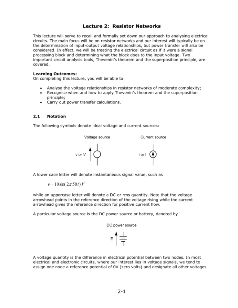
Lecture 2: Resistor Networks This lecture will serve to recall and formally set down our approach to analysing electrical circuits. The main focus will be on resistor networks and our interest will typically be on the determination of input-output voltage relationships, but power transfer will also be considered. In effect, we will be treating the electrical circuit as if it were a signal processing block and determining what the block does to the input voltage. Two important circuit analysis tools, Thevenin’s theorem and the superposition principle, are covered. Learning Outcomes: On completing this lecture, you will be able to: 2.1 Analyse the voltage relationships in resistor networks of moderate complexity; Recognise when and how to apply Thevenin’s theorem and the superposition principle; Carry out power transfer calculations. Notation The following symbols denote ideal voltage and current sources: Voltage source Current source i or I v or V A lower case letter will denote instantaneous signal value, such as v 10 sin( 2 50 t ) V while an uppercase letter will denote a DC or rms quantity. Note that the voltage arrowhead points in the reference direction of the voltage rising while the current arrowhead gives the reference direction for positive current flow. A particular voltage source is the DC power source or battery, denoted by DC power source E A voltage quantity is the difference in electrical potential between two nodes. In most electrical and electronic circuits, where our interest lies in voltage signals, we tend to assign one node a reference potential of 0V (zero volts) and designate all other voltages 2-1 with respect to this 0V reference node. Such a 0V reference is termed a ground and carries the symbol The following diagram illustrates two ways of working with a 5V battery, itself shown in Fig (a): 0V +5 V 5V 5V 5V 0V (a) -5 V (b) (c) In Fig (b) the lower node is grounded resulting in a potential of +5V on the upper node; in Fig (c) the upper node is grounded resulting in a potential of -5V on the lower node. 2.2 Device Characterisation I I D V R D I V R V The electrical operation of any electronic device is captured by means of the relationship between the current I flowing through the device in response to a voltage V across the device. For most electronic devices this relationship is non-linear, such as illustrated for device D above. For the device known as a resistor, the relationship (at a given temperature) is linear. This linear relationship is expressed by Ohm’s Law: I 1 V R where R is the resistance value given in ohms. 2-2 Where we have a circuit with multiple devices — resistors for the present — we make use of Kirchhoff’s laws to analyse the circuit. In building up these multi-device circuits, there are only two possibilities for configuring the devices: putting them in series or putting them in parallel. (i) Resistors in Series: I R1 V1 R2 V2 VS Noting that the same current I flows in each resistor, the voltage drops are given V1 R1 I and V2 R2 I Applying Kirchhoff’s Voltage Law to the loop, we get VS V1 V2 I R1 R2 Noting that VS is the voltage across the series resistor combination and I is the current through the series combination, we have RSERIES VS R1 R2 I Resistors in series add. (ii) Resistors in Parallel: I I1 VS R1 I2 V1 R2 Noting that the same voltage is dropped across each resistor 2-3 V2 VS V1 V2 the individual currents can be expressed I1 V1 VS R1 R1 and I2 V2 VS R2 R1 Applying Kirchhoff’s Current Law we get I I1 I 2 VS VS R1 R2 VS R1 R2 R1 R2 Again noting that VS is the voltage across the parallel resistor combination and I is the current flowing through the combination, we can express the effective resistance value by RPAR 2.2 VS RR 1 2 I R1 R2 Voltage Dividers Consider applying an input voltage Vi to a series resistor combination R1 and R2, and taking as output Vo the voltage across R2: V1 I1 R1 Vi As before I1 I 2 I With Vi I R1 R2 I2 R2 and Vo I R2 The output-input relationship is given by 2-4 Vo Vo R2 I R2 Vi R1 R2 I R1 R2 This basically states that the output is a scaled replica of the input with the scale factor being a fraction determined by the resistor ratio R2/(R1+R2). The following example illustrates a practical application of this circuit model. Example 2.1: microphone amplifier RS Vo VS RL Vo Consider the electrical connection between a microphone and an amplifier. The microphone is modelled by a non-ideal voltage source (comprising an ideal voltage source VS and a source resistance RS) while from the point of view of the microphone the amplifier appears as a resistive load RL. The voltage signal actually going in to the amplifier is given by VO RL VS RS R L Usually we would wish to get as much signal as possible into the amplifier and this clearly requires RL RS 2.3 Thevenin’s Theorem Consider the following circuit. R1 VS R2 Vo RL Noting that the two resistors R2 and RL can be combined in parallel into an equivalent resistor RPAR R2 R L R2 R L we can express the output voltage by 2-5 RPAR R1 RPAR VO R2 R L R2 R L VS VS R2 R L R1 R2 R L R2 RL VS R1 R2 R1 RL R2 RL RL R2 VS R1 R2 RL R1 R2 RL R2 VS R1 R2 R1 R2 RL R1 R2 If we make the following substitutions: Let RT R1 R2 R1 R2 and VT R2 VS R1 R2 We can express the output as VO RL VT RT RL It is as if we had replaced all the circuit to the left of RL by a voltage source VT and a resistor RT: RT Vo VT RL This is the essence of what is known as Thevenin’s theorem which states: Any part of a linear electrical circuit can be replaced by a single voltage source V T and a source resistor RT. The Thevenin voltage source VT can be determined by calculating the open circuit voltage for that part of the overall circuit being replaced. The Thevenin resistance RT can be determined by calculating the overall resistance looking back into that part of the overall circuit being replaced and putting any voltage (or current) source to zero. Looking again at our original circuit 2-6 R1 R2 VS Vo RL what we want to do is to replace that part of the circuit to the left of the V O arrow: R1 VT R2 VS RT For this sub-circuit, clearly the open circuit voltage is given by VT R2 VS R1 R2 If we now put VS to zero and look back into the sub-circuit we get R1 R2 RT showing that RT is indeed the parallel combination of R1 and R2 RT 2.4 R1 R2 R1 R2 The Superposition Principle Consider the following voltage divider: V1 V2 I1 I2 R1 R2 Vo VS1 2-7 VS2 The problem is to determine the dependency of the output voltage V O on the two voltage sources VS1 and VS2. The designated currents I1 and I2 may be expressed I1 V1 VS1 VO R1 R1 I2 From Kirchhoff’s current law, we have V2 VS 2 VO R2 R2 I1 I 2 giving VS1 VO V VO S2 R1 R2 VS1 VS 2 VO VO R1 R2 R1 R2 VO R2 R1 VS1 R2 VS 2 R1 R2 R1 R2 R1 VO R2 R1 VS 1 VS 2 R1 R2 R1 R2 An alternative means of arriving at this result is based on the superposition principle. Basically the principle states: In a linear circuit, if a node voltage VO depends on a number of independent voltage sources, say VS1 and VS2, then Calculate the node voltage due to the first source with all other sources zeroed; Calculate the node voltage due to the second source with all other sources zeroed; etc. The overall node voltage is then the sum of the individual values as calculated above. In the case of our example, VO VO VS1 , VS 2 0 VO VS 2 , VS1 0 VO VS1 VO VS 2 for short. VO(VS1) may be determined from the following diagram: R1 Putting VS2 = 0V R2 VO(VS1) VS1 From our consideration of voltage dividers we have 2-8 VO VS1 R2 VS 1 R1 R2 VO(VS2) may be determined from R1 R2 VO(VS2) Putting VS1 = 0V VS2 Again voltage divider consideration shows VO VS 2 R1 VS 2 R1 R2 The superposition principle now gives VO VO VS1 VO VS 2 2.5 R2 R1 VS1 VS 2 R1 R2 R1 R2 as before. Power Transfer Sometimes when connecting a non-ideal signal source (ie a signal source with a non-zero source resistance) to a resistive load we are primarily interested in delivering as much power as possible to the load rather than trying to keep the signal level as high as possible. We now investigate the requirements for maximising the transfer of average power. RS Vs RL Vl Assume the signal quantities are rms quantities to facilitate average power calculations. The average power delivered to the load is Pl Vl 2 RL 2-9 1 RL RL Vs RS R L RL R S R L 2 2 Vs2 The question now is: for a given source (ie known Vs and RS), what value of RL maximises Pl? Differentiating Pl with respect to RL we obtain dPl 3 2 RL 2RS RL RS RL 1 Vs2 dRS Vs2 RS RL 2RL RS RL 3 Vs2 RS RL RS RL 3 0 R L RS for a maximum for maximum power transfer. That is, the load resistance should be chosen to equal the source resistance to maximise the power transfer from source to load. 2.6 Concluding Remarks In this lecture, necessary and important aspects of electrical circuit theory have been reviewed and a consistent system of notation has been set out. The particular methods of analysis used here are not the only methods to arrive at the desired solution or relationship — in many practical problems, there will be different possible approaches to the solution; what has been provided here is a set of approaches. 2-10
