PowerPoint-Präsentation
advertisement
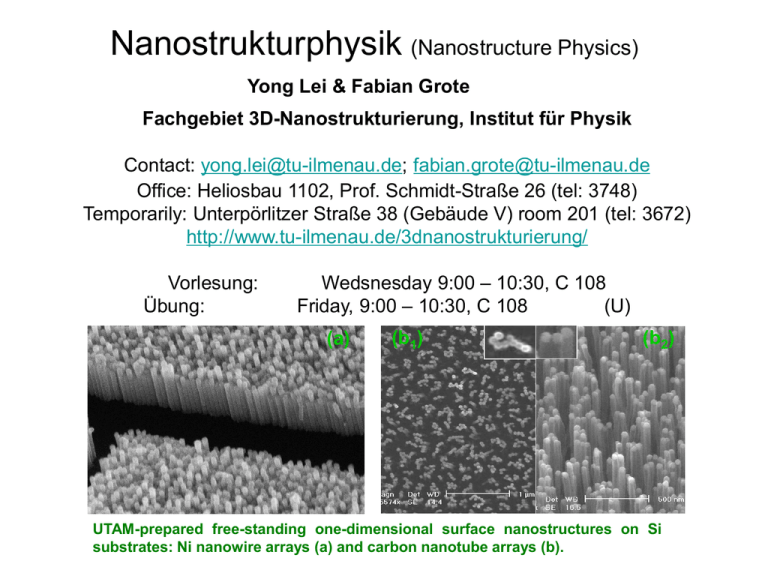
Nanostrukturphysik (Nanostructure Physics) Yong Lei & Fabian Grote Fachgebiet 3D-Nanostrukturierung, Institut für Physik Contact: yong.lei@tu-ilmenau.de; fabian.grote@tu-ilmenau.de Office: Heliosbau 1102, Prof. Schmidt-Straße 26 (tel: 3748) Temporarily: Unterpörlitzer Straße 38 (Gebäude V) room 201 (tel: 3672) http://www.tu-ilmenau.de/3dnanostrukturierung/ Vorlesung: Übung: Wedsnesday 9:00 – 10:30, C 108 Friday, 9:00 – 10:30, C 108 (U) (a) (b1) (b2) UTAM-prepared free-standing one-dimensional surface nanostructures on Si substrates: Ni nanowire arrays (a) and carbon nanotube arrays (b). Contents of Class 6 Optical properties of 1-D nanostructures Features of optical properties of 1-D nanostructures • Sharp and discrete features in absorption spectra & ‘‘band-edge’’ PL shift and enhancement – results of quantum confinement effects. • Anisotropic PL, highly polarized along axial direction – the large dielectric contrast between nanowire and surrounding environment. • Efficient migration of electrons and holes to surface of nanostructures allows them to participate in chemical reactions before recombining – enhance the efficiency of solar cells. • Nanowires with optical properties tuned by changing aspect ratio. • Single crystalline and well faceted nanowires can function as effective resonance cavities; the lasing properties. • Oxygen vacancies and chemical surface absorption plays an important role to photo-sensitivity and PL of oxide 1-D nanostructures. 1st finding (obvious evidence) of the quantum confinement effect of 1-D nanostructures: Holmes JD, Science, 2000. Defect-free Si nanowires with uniform diameters ranging from 4 to 5 nm and length of several micrometers by a supercritical solution-phase approach. Si nanowires synthesized at 500 oC (in hexane) at pressures of 200 bar (A and B) and 270 bar (C and D). The nanowires are highly crystalline. In both (B) and (D), the lattice fringes are Si (111) planes, separated by 3.14 Ǻ. The absorption edge of the Si nanowires was strongly blue-shifted from the bulk indirect band gap of 1.1 eV and showed sharp discrete absorption features and strong band-edge PL, results from quantum confinement effects. The 100> oriented wires have a much higher exciton energy than that of the 110> oriented wires. Band-Gap Variation of Size- and Shape-Controlled CdSe Quantum Rods (Li LS, Nano Letters, 2001) TEM images of 4 CdSe nanorod samples. The scale bar is 50 nm. PL spectra of 3.7 nm wide CdSe rods with lengths: 9.2, 11.5, 28.0, 37.2 nm, respectively (from left to right), excited at 450 nm. Band gap of CdSe quantum rods vs length and width viewed from two different angles. The data are fit in 1/length (1/L), 1/width (1/W), and aspect ratio (L/W). The surface of best fit obtained is: 1.8563 -2.0835/L2 + 4.5507/W2 - 0.0018(L/W)2 + 0.0001(L/W)3 + 10.5824/L3 0.3833/W3. Quantum confinement observed in ZnO/ZnMgO multiple quantum well nanorod heterostructures (Park WI, Advanced Materials, 2003) 10 periods of Zn0.8Mg0.2O/ZnO on ZnO nanorods. A: 1.1 nm wells and B: 2.5 nm wells. Quantum confinement in 1-D nanostructures Quantum confinement is approximately described by simple particle-in-a-box type models, and its most distinctive signature is 1/dn (d: diameter, 1 ≤ n ≤ 2) size dependence of bandgap. The quantum confinement effect in semiconductor nanodots and nanowires did not exactly follow the particle-in-a-box prediction. A particle-in-a-cylinder mode: The calculated energy shift ΔE, relative to the bulk band gap as a function of the nanowire radius R, is given by: L is the length of the cylinder, m* is the reduced effective exciton mass (memh /(me + mh)), ħ is Planck’s constant, e is the electron charge. The first term represents the size-dependent kinetic energy confinement imposed by the walls of the nanowire cylinder. The second term is the attractive Coulomb interaction between electron and hole in perturbation theory. This mode provides excellent fits to experimental results. Nanowire Lasing (Yang PD‘s group) Nanowires with flat end facets can be used as optical resonance cavities to generate coherent light. UV lasing at RT has been demonstrated for ZnO and GaN nanowires with epitaxial arrays and single nanowires. ZnO and GaN are wide bandgap semiconductors (3.37, 3.42 eV) suitable for UV-blue optoelectronics. The large binding energy for excitons in ZnO (∼60 meV) permits lasing via exciton-exciton recombination at low excitation conditions. GaN has an electron-hole plasma lasing mechanism. Well-faceted nanowires with diameters from 100 to 500 nm support axial Fabry-Perot waveguide modes: Δλ = λ2/[2Ln(λ)], where L is the cavity length and n(λ) is the group index of refraction owing to the large diffraction losses. Diffraction prevents smaller wires from lasing: PL is lost instead to the surrounding radiation field. ZnO and GaN nanowires produced by VLS growth are cavities with low intrinsic finesse (F) owing to the low reflectivity (R) of their end facets (∼19%): F = πR1/2/(1-R)] the confinement time for photons is short and photons travel an average of 1 to 3 half-passes before escaping from the cavity. Nanowire Lasing The transition from spontaneous PL to lasing is achieved by exciting high density of wires via pulsed UV illumination. The dependence of nanowire emission on pump power has 3 regions: (a) spontaneous emission, (b) stimulated emission (lasing starting) above a certain threshold, (c) saturation (lasing) at high pump power. The lasing thresholds vary several orders of magnitude as a consequence of different nanowire dimensions, the lowest threshold observed for ZnO is ∼70 nJ cm-2 and for GaN ∼500 nJ cm-2. The spectral position of the lasing is independent of pump power but shows significant red-shift near saturation. GaN nanowires show a consistent red-shift from threshold to saturation. (a) Spectra of light emission from GaN/AlGaN core-shell nanowires below, near and above lasing threshold (about 2–3 µJ/cm2). (b) The power dependence of output integrated emission intensity. Far-field imaging indicates that PL and lasing emission are localized at the ends of nanowires, which suggests strong waveguide behavior that is consistent with axial Fabry-Perot modes. spontaneous emission stimulated emission (lasing) The ultrafast dynamics of the lasing in ZnO nanowires and nanobelts Transient PL spectroscopy has been used to detect carrier relaxation dynamics near the lasing threshold. (a) SEM of as-grown nanowire array and (b) single nanowire dispersed on sapphire substrate. Inset: far-field image of nanowire emission. (c) SEM of as-grown nanbelts and (d) single dispersed belt on silicon. Inset: far-field image of belt lasing emission. The ultrafast dynamics of the lasing in ZnO nanowires and nanobelts Above the lasing threshold, a bi-exponential decay of the PL was observed, with a fast component (∼10 ps) corresponding to exciton-exciton lasing and a slow component (∼70 ps) owing to free-exciton spontaneous emission. (a) PL/lasing spectra of single ZnO nanowire near the lasing threshold (excitation ∼1 µJ/cm2) and (b) transient PL response. Long decay component is about 70 ps and short component is about 9 ps (red) and 4 ps (black). Nanowire Lasing The useful applications for nanowire lasers require that they be integrated in circuits and activated by electron-injection rather than optical pumping. Lieber and coworkers have made progress in this direction by assembling n-type CdS nanowire (Fabry-Perot cavities) on p-Si wafers to form the required heterojunction for electrically driven lasing: Single-nanowire electrically driven lasers (Lieber et al., Nature 2003) First, optical-pumped Single-nanowire lasers a, A nanowire as an optical waveguide, with cleaved ends of a Fabry–Perot cavity. b, SEM image of a cleaved CdS nanowire end. c, RT PL image of a CdS nanowire excited (low-left corner, power 10 mW) about 15 mm away from the nanowire end. The white arrow highlight the nanowire end. d, PL spectra obtained from the body of the nanowire (blue) and the end of the nanowire (green) at low pump power (10 mW). e, Spectrum from the nanowire end at higher pump power (80 mW) exhibiting periodic intensity variation. Optically pumped nanowire laser: a, Emission spectra from a CdS nanowire end with a pump power of 190, 197 and 200 mW (red, blue and green) recorded at 8 K. b, Emission intensity and FWHM of emission peaks versus laser pump power. The emission intensity from nanowire body (blue) maintains a low value, whereas the emission from nanowire end (green) shows superlinear behavior above 125 mW. The FWHM (red) has a nearly constant value of about 12 nm at low power, and narrows to the instrument-resolution value at high power. Single-nanowire electrical-driven lasers To investigate nanowire injection lasers, a hybrid structure was used: n-type CdS nanowire laser cavities are assembled onto p-Si electrodes defined in heavily p-doped planar substrates. An image of a typical device is shown in b. Images of the RT electroluminescence produced in forward bias from these hybrid structures (b) exhibit strong emission from the exposed CdS nanowire ends. (d) At low injection currents the spectrum of end emission shows a broad peak, consistent with spontaneous emission. Above 200mA threshold, the spectrum quickly collapsed into a few very sharp peaks with a dominant emission at 509.6 nm. These sharp peaks come from both spontaneous and stimulated emission, and had an average spacing of about 1.8 nm. The multiple peaks versus a single mode is often observed when lasing in planar devices pumped close to threshold. (e) Low-T measurements on independent CdS injection laser devices clearly show that the spontaneous emission spectrum can collapse to a sharp peak of lasing, the results are very similar to the low-temperature optically pumped results. Techniques for device fabrication of semiconductor lasers is costly and difficult to integrate directly with Si microelectronics. There are considerable interest in using organic molecules, polymers, and inorganic nanostructures for lasers, because these materials can be integrated into devices by chemical processing. And stimulated emission or lasing have been reported for optically pumped inorganic nanowires and organic systems. Electrical-driven nanowire lasers might be assembled in arrays capable of emitting a wide range of colors, used in flat displays. Field-emission Display (FED) Since the discovery of CNTs, much attention has been paid to explore the usage of inorganic semiconductor 1-D nanostructures as field-emitters: low work functions, high aspect ratios, high mechanical stabilities, high electrical and thermal conductivities. Field-emission is one of the main features of nanostructures, and is of great commercial interest in FEDs and other electronic devices. Recent progress in the synthesis and assembly of nanostructures has resulted in a considerable increase in the current density and lowering of turn-on voltage. Besides CNTs, some other inorganic semiconductor nanostructures used for fieldemitters, such as ZnO, Si, WO3, SiC, ZnS, AlN. Field-emission (Fowler–Nordheim tunneling) is a quantum tunneling process in which electrons pass from an emitting material (negatively biased) to the anode through a barrier (vacuum) in the presence of a high electric field. This phenomenon is highly dependent both on properties of the material and the shape of cathode, and the materials with higher aspect ratios and sharp edges (nanowires or nanotubes) produce higher field-emission currents. The current density J produced by an electric field E (the Fowler–Nordheim equation): J = (Aβ2E2/ø)exp(-Bø3/2/βE), I = S × J, E = V/d, or ln(J/E2) = ln(Aβ2/ø) – Bø3/2/βE, (1) (2) (A: 1.54 × 10⁻⁶ A eV V-2, B: 6.83 × 10³ eV-3/2 V μm-1, S: emitting area, V: applied potential, I: emission current, β: field enhancement factor, d: distance between sample and anode, ø: work function) β is related to emitter geometry and crystal structure, and spatial distribution of emitting centers, can be expressed approximately as β = h/r, (h is the height and r is radius of curvature of an emitting center). Materials with elongated geometry and sharp tips or edges can greatly increase an emission current. The emission current is strongly dependent on three factors: (i) work function of an emitter surface, (ii) radius of curvature of the emitter end, (iii) emission area. A lower work function material can produce a higher electron emission current. However, not all low work function materials are ideal for constructing field-emission cathodes (a) The emission occurs from tip of an emitter. (b) The emitter can have different emission currents depending upon the tip geometry, such as (i) round tip, (ii) blunt tip and (iii) conical tip. (W. Z. Wang, et al., Adv. Mater., 2006) For a given material, emission current can be enhanced through increasing its aspect ratio, assembling it into arrays, or decorating its surface with a lower work function material. ZnO 1-D nanostructures (belts and wires) Aligned ultra-long ZnO nanobelts. (a) optical photo of nanobelts with length of several mm. SEM (b) indicates beltlike structures with a width up to 6 μm. (c) TEM image of a single belt. Its transparency to electron beam (can see a copper TEM grid beneath belt) clearly reflects much smaller thickness of belts compared to widths. The HRTEM image of this belt is shown in (d) shows the perfect crystallinity and defect-free nature of nanobelts. (Wang WZ, Adv Mater, 2006) Field-emission performances of aligned ultralong ZnO nanobelts. (a) is a typical field emission current density–applied field (J–F) curve. The turn-on electric field is about 1.3 V μm-1. (b) shows the Fowler–Nordheim plot for the nanobelts, which fits well to the linear relationship given by Fowler–Nordheim equation: ln(J/E2) = ln(Aβ2/ø) – Bø3/2/βE From the slope of fitted straight line in (b), the ZnO nanobelts have a very high fieldenhancement factor of 1.4 × 10⁴, which is the result of the extremely high aspect ratio of the emitter geometry. ZnS nanobelt quasi-arrays ZnS nanobelt quasi-arrays. The length of belts is about several hundreds of micrometers; some of them may even be as long as a millimeter. These nanobelts form in bundles. Within a bundle they are quasi-aligned. In many cases even perfectly parallel ensembles are visible. The electron diffraction patterns show the similar orientation of nanobelts along the [001] direction. HRTEM images of an individual belt display the defect-free (001) lattice plane of wurtzite Zn and confirm the [001] growth direction. The orientation-ordered ZnS nanobelt quasi-arrays have much improved fieldemission properties as compared to random nanowires: a low turn-on field (~ 3.55 V μm-1) and a high field-enhancement factor (~ 1850). The emission current density of ~ 14.6 mA cm-2 at a field of 5.5 V μm-1 for quasi-aligned ZnS nanobelt arrays is more than 20 times higher than that of randomly distributed ZnS nanobelts of ~ 0.68 mA cm-2 at the same field. Some effective routes were developed to enhance the field-emission performances: e.g. only ~ 1 V μm-1 turn-on field at a 3 mA cm-2 current density was achieved from ultra-sharp (~ 1 nm diameter) and ultra-high density (109 – 3 × 1011 cm-2) SiCcapped Si nanotip arrays. SiC-capped silicon nanotips: (a) nanotips of about 1 μm height with an aspect ratio of about 1000; (b) the high density nature of nanotip arrays. (c) TEM image of a SiC-capped Si nanotip. The inset is a magnified lattice image at the interface between the Si and SiC. (Lo HC, Appl Phys Lett, 2003) A typical field emission data obtained from SiC-capped silicon nanotips demonstrating ultralow turn-on electric fields (only ~ 1 V μm-1 turn-on field at a 3 mA cm-2 current density). The inset presents the emission current data plotted in the Fowler– Nordheim coordinates, wherein the dashed line represents a linear relationship for an ideal field emitter. WO3 1-D nanostructures (Chen J, Appl Phys Lett, 2007) A FED using WO3 nanowires as cathode material, based on a double-gate structure: a cathode and a gate plate. Cathode plate consists of nano-emitters grown on a substrate. Anode is a phosphor screen. Gate plate is a ceramic plate with round apertures. Metallic strips were prepared on both sides of ceramic plate (perpendicular to each other while electrically insulated by ceramic). 8 × 8 arrays of WO3 nanowires on a Si wafer (a). The diameter of each cathode is ~ 1 mm, the distance between the pixels is 2.5 mm. The dark spots on the anode correspond to the pixels (b). The functioning of the device, where Arabic and Chinese characters appear by switching of individual spots. Each pixel could be accurately addressed without any interference. Three-Dimensional Surface Nano-Patterning (a1) (b1) (a2) (b2) Addressing of an individual 1-D nanostructure (a) (d) (b) (c) (e) (f) The addressing system (3 × 3 array instead of 10 × 10 array): (a) Pt lines on a substrate; (b) an Al layer with the pre-patterns of an array of shallow nano-holes; (c) anodization process to prepare alumina mask with through-channels down to the Pt lines; (d) synthesize nanowires; (e) Pt lines on the top followed with the preparation of a supporting layer; (f) removal of the mask. Two sets of Pt lines are indexed. Nanowire with an arrow mark is indexed as ‘1A’. Thank you and have a nice day! Lab Tour (Thursday afternoon) Next course: Vorlesung: June 28 (Wed), 9:00 – 10:30, C 108 Übung: June 30 (Fri), 9:00 – 10:30, C 108 (U)
