Ch4
advertisement
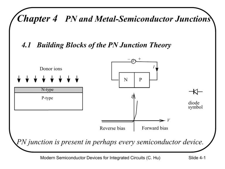
Chapter 4 PN and Metal-Semiconductor Junctions 4.1 Building Blocks of the PN Junction Theory – V + I Donor ions N P N-type I P-type diode symbol V Reverse bias Forward bias PN junction is present in perhaps every semiconductor device. Modern Semiconductor Devices for Integrated Circuits (C. Hu) Slide 4-1 4.1.1 Energy Band Diagram of a PN Junction N-region P-region Ef (a) Ef is constant at equilibrium Ec (b) Ec Ef Ev Ec and Ev are known relative to Ef Ev Ec Ef Ev (c) Neutral N-region Depletion layer Neutral P-region Ec (d) Ef Ev Ec and Ev are smooth, the exact shape to be determined. A depletion layer exists at the PN junction where n 0 and p 0. Modern Semiconductor Devices for Integrated Circuits (C. Hu) Slide 4-2 4.1.2 Built-in Potential (a) N-type P-type NNdd (b) q NNa a Ec fbi Ef Ev V fbi (c) xN 0 xP x Can the built-in potential be measured with a voltmeter? Modern Semiconductor Devices for Integrated Circuits (C. Hu) Slide 4-3 4.1.2 Built-in Potential N-region n Nd Nce q A kT kT N c A ln q Nd 2 ni kT N c N a q B kT P-region n Nce B ln 2 Na q ni Nc kT N c N a ln fbi B A ln 2 q Nd ni fbi kT N d N a ln 2 q ni Modern Semiconductor Devices for Integrated Circuits (C. Hu) Slide 4-4 4.1.3 Poisson’s Equation Gauss’s Law: s: permittivity (~12o for Si) : charge density (C/cm3) E (x) E (x + Dx) Dx x Poisson’s equation Modern Semiconductor Devices for Integrated Circuits (C. Hu) Slide 4-5 4.2 Depletion-Layer Model (a) N (b) 4.2.1 Field andN Potential in the Depletion Layer P N d a N eut ra l Re gion D eple tion L a yer N e utr al R egi on N P xnN xpP 0 On the P-side of the depletion layer, = –qNa d E qN a s dx qNd xpP (c) xnN x –qN a E ( x) (d) xnN f bi qN a s x + C1 qN a s ( x P x) On the N-side, = qNd (e) E ( x) x pP 0 x qN d s ( x - xN ) V Modern Semiconductor Devices for Integrated Circuits (C. Hu) Slide 4-6 (a) (b) P N N d Potential in theNDepletion 4.2.1 Field and Layer a N eut ra l Re gion N D eple tion La yer –xnN N e utral R egi on P xpP 0 The electric field is continuous at x = 0. qN Nda |xP| = Nd|xP| (c) xp Which side –x of the junction is depleted more? x n –qNa A one-sided junction is called a N+P junction or P+N junction Modern Semiconductor Devices for Integrated Circuits (C. Hu) Slide 4-7 qNd xp (c) 4.2.1x Field–qNand Potential in the Depletion Layer x n a On the P-side, (d) xn N x pP 0 x Arbitrarily choose the voltage at x = xP as V = 0. V f bi (e) xnN xpP x Ec fbi , qNa V ( x) ( xP x ) 2 2 s built-in potential (f) Ef Ev On the N-side, qNd V ( x) D ( x xN )2 2 s qNd fbi ( x xN )2 2 s Modern Semiconductor Devices for Integrated Circuits (C. Hu) Slide 4-8 (a) N Nd P Na 4.2.2 Depletion-Layer Width (b) N eut ra l Re gion N D eple tion La yer –xnN N e utral R egi on P xpP 0 V is continuous at x = 0 xP xN Wdep d If Na >> Nd , as in a P+NqN junction, (c) Wdep 2 sfbi q xp 2 sfbi –xxn N qN d –qN a |x P||xN|N d 1 1 + Na Nd x Na @ 0 What about a N+P junction? Wdep 2 s fbi qN where 1 1 1 1 + N N d N a lighter dopantdensity (d) Modern Semiconductor Devices for Integrated Circuits (C. Hu) –xn 0 xp Slide 4-9 x EXAMPLE: A P+N junction has Na=1020 cm-3 and Nd =1017cm-3. What is a) its built in potential, b)Wdep , c)xN , and d) xP ? Solution: a) kT N d N a 1020 1017 cm6 fbi ln 0.026V ln 1V 2 20 6 q ni 10 cm 1/ 2 b) W 2 sfbi 2 12 8.8510 1 dep 1.6 1019 1017 qNd 14 0.12 μm c) xN Wdep 0.12 μm d) xP xN Nd Na 1.2 104 μm 1.2 Å 0 Modern Semiconductor Devices for Integrated Circuits (C. Hu) Slide 4-10 4.3 Reverse-Biased PN Junction + V – N P Ec qfbi Ec Ef Ev Ef Ev (a) V = 0 Ec qfbi + qV Ec Efn qV Efp Ev Wdep 2 s (fbi + | Vr |) 2 s potentialbarrier qN qN 1 1 1 1 + N N d N a lighter dopant density • Does the depletion layer widen or shrink with increasing reverse bias? Ev (b) reverse-biased Modern Semiconductor Devices for Integrated Circuits (C. Hu) Slide 4-11 4.4 Capacitance-Voltage Characteristics N Nd Conductor P Na Insulator Conductor Wde p Reverse biased PN junction is a capacitor. s Cdep A Wdep • Is Cdep a good thing? • How to minimize junction capacitance? Modern Semiconductor Devices for Integrated Circuits (C. Hu) Slide 4-12 4.4 Capacitance-Voltage Characteristics 1/C dep 2 1 Cdep 2 Wdep 2 A 2 s 2 Capacitance data 2(fbi + V ) qN S A2 Slope = 2/qN s A2 – fbi Vr Increasing reverse bias • From this C-V data can Na and Nd be determined? Modern Semiconductor Devices for Integrated Circuits (C. Hu) Slide 4-13 EXAMPLE: If the slope of the line in the previous slide is 2x10²³ F-2 V-1, the intercept is 0.84V, and A is 1 mm2, find the lighter and heavier doping concentrations Nl and Nh . Solution: N l 2 /( slope q s A2 ) 2 /(2 1023 1.6 1019 12 8.851014 108 cm2 ) 6 1015 cm3 2 qf 0.84 kT N h N l ni kTbi 1020 0.026 18 3 fbi ln 2 N h e e 1 . 8 10 cm q ni Nl 6 1015 • Is this an accurate way to determine Nl ? Nh ? Modern Semiconductor Devices for Integrated Circuits (C. Hu) Slide 4-14 4.5 Junction Breakdown I Forward Current V B, breakdown voltage V R Small leakage Current A P N R A C 3.7 V Zener diode B IC D A Zener diode is designed to operate in the breakdown mode. Modern Semiconductor Devices for Integrated Circuits (C. Hu) Slide 4-15 4.5.1 Peak Electric Field N+ Na 0 Neutral Region increasing reverse bias P xp 2qN (fbi + | Vr |) Ep E (0) s (a) E Ep 1/ 2 increasing reverse bias xp x VB s Ecrit 2 2qN fbi (b) Modern Semiconductor Devices for Integrated Circuits (C. Hu) Slide 4-16 4.5.2 Tunneling Breakdown Dominant if both sides of a junction are very heavily doped. Filled States - Empty States Ec Ev J Ge H / εp I V Ep Ecrit 106 V/cm Breakdown Modern Semiconductor Devices for Integrated Circuits (C. Hu) Slide 4-17 4.5.3 Avalanche Breakdown Ec original electron Efp Ev • impact ionization: an energetic electron generating electron and hole, which can also cause impact ionization. • Impact ionization + positive feedbackavalanche breakdown VB electron-hole pair generation Ec Efn s Ecrit 2 2qN 1 1 1 VB + N Na Nd Modern Semiconductor Devices for Integrated Circuits (C. Hu) Slide 4-18 4.6 Forward Bias – Carrier Injection Forward biased Forward biased VV=0 =0 V I=0 – + Ec N qfbi P - Ef Ev Ec qfbi –qV Ef n qV Efp Ev + Drift and diffusion cancel out Minority carrier injection Modern Semiconductor Devices for Integrated Circuits (C. Hu) Slide 4-19 4.6 Forward Bias – Quasi-equilibrium Boundary Condition n( xP ) Nce ( Ec E fn ) / kT Nce ( Ec E fp ) / kT ( E fn E fp ) / kT e ( E fn E fp ) / kT EEcc nP0e nP0e qV / kT • The minority carrier EEfnfnfn fp EEfp EEv v xx densities are raised by eqV/kT • Which side gets more carrier injection? xN0 x0 P N P Modern Semiconductor Devices for Integrated Circuits (C. Hu) Slide 4-20 4.6 Carrier Injection Under Forward Bias– Quasi-equilibrium Boundary Condition qV n(xP ) nP 0 e p (xP) p N 0 e kT 2 ni qV e Na kT 2 qV kT ni qV e Nd n( xP ) n( xP ) nP0 nP0 (eqV kT kT p( xN ) p( xN ) pN 0 pN 0 (eqV 1) kT 1) Modern Semiconductor Devices for Integrated Circuits (C. Hu) Slide 4-21 EXAMPLE: Carrier Injection A PN junction has Na=1019cm-3 and Nd=1016cm-3. The applied voltage is 0.6 V. Question: What are the minority carrier concentrations at the depletion-region edges? Solution: n( xP ) nP0eqV kT 10 e0.6 0.026 1011 cm-3 p( xN ) pN 0eqV kT 104 e0.6 0.026 1014 cm-3 Question: What are the excess minority carrier concentrations? Solution: n( xP ) n( xP ) nP0 1011 10 1011 cm-3 p( xN ) p( xN ) pN 0 1014 104 1014 cm-3 Modern Semiconductor Devices for Integrated Circuits (C. Hu) Slide 4-22 4.7 Current Continuity Equation A a a re J p ( x) q A J p ( x + Dx) + A Dx q p A Jp (x) Jp (x + Dx) p Volume = A·Dx Dx J p ( x + Dx) J p ( x) Dx dJ p dx q q p p x Modern Semiconductor Devices for Integrated Circuits (C. Hu) Slide 4-23 4.7 Current Continuity Equation dJ p dx q p Minority drift current is negligible; Jp= –qDpdp/dx d2p p qDp 2 q dx p d p p p 2 2 dx Dp p Lp 2 d 2 n n 2 2 dx Ln Lp and Ln are the diffusion lengths L p D p p Ln Dn n Modern Semiconductor Devices for Integrated Circuits (C. Hu) Slide 4-24 4.8 Forward Biased Junction-- Excess Carriers P + N d 2 p p 2 2 dx Lp xP -x N 0 x p() 0 p( xN ) pN 0 (eqV / kT 1) x / Lp x / Lp p ( x) Ae + Be x xN / L p qV / kT p ( x) pN 0 (e 1)e , x xN Modern Semiconductor Devices for Integrated Circuits (C. Hu) Slide 4-25 4.8 Excess Carrier Distributions 1.0 P-side N-side Na = 1017 cm -3 nP ' ex /L n Nd = 21017 cm-3 – 3L n –2L n 0.5 –Ln pN ' e–x /L p 0 L p 2L p 3L p 4Lp x xN / L p qV / kT p ( x) pN 0 (e 1)e , x xN n( x) nP0 (eqV / kT 1)e x xP / Ln , x xP Modern Semiconductor Devices for Integrated Circuits (C. Hu) Slide 4-26 EXAMPLE: Carrier Distribution in Forward-biased PN Diode N-type Nd = 5 cm-3 Dp =12 cm2/s p = 1 ms P-type Na = 101 7 cm-3 Dn=36.4 cm2 /s n = 2 ms • Sketch n'(x) on the P-side. n( xP ) nP 0 (eqV 2 ni 1020 0.6 0.026 kT qV / kT 1) (e 1) 17 e 1013 cm3 Na 10 N-side 1013cm-3 P-side n’ ( = p’ ) 2 p´ ( = n’ ) 2´ Modern Semiconductor Devices for Integrated Circuits (C. Hu) x Slide 4-27 EXAMPLE: Carrier Distribution in Forward-biased PN Diode • How does Ln compare with a typical device size? Ln Dn n 36 2 10 6 85 μm • What is p'(x) on the P- side? Modern Semiconductor Devices for Integrated Circuits (C. Hu) Slide 4-28 4.9 PN Diode I-V Characteristics Jtotal Jtotal Jn = Jtotal – Jp Jp = Jtotal – Jn JnP JnP JpN JpN x P-side 0 J pN N-side P-side Dp dp( x) qDp q pN 0 (eqV dx Lp J nP qDn D dn( x) q n nP 0 (e qV dx Ln kT kT 0 1)e N-side x x N L p 1)e x xP Ln Dp qV Dn T otalcurrent J pN ( x N ) + J nP ( xP ) q p +q n P 0 ( e L N0 Ln p J at all x Modern Semiconductor Devices for Integrated Circuits (C. Hu) kT 1) Slide 4-29 The PN Junction as a Temperature Sensor I I 0 (eqV kT 1) Dp Dn I 0 Aqni + L N p d Ln N a 2 What causes the IV curves to shift to lower V at higher T ? Modern Semiconductor Devices for Integrated Circuits (C. Hu) Slide 4-30 4.9.1 Contributions from the Depletion Region n p ni eqV / 2kT Net recombination (generation) rate: ni qV / 2 kT (e 1) dep I I 0 (e qV / kT 1) + A qniWdep τ dep (eqV / 2kT 1) Space-Charge Region (SCR) current I leakage I 0 + A qniWdep τ dep Under forward bias, SCR current is an extra current with a slope 120mV/decade Modern Semiconductor Devices for Integrated Circuits (C. Hu) Slide 4-31 4.10 Charge Storage 1013 cm -3 N-side QI P-side I Q s Q I s n' p’ 22 x What is the relationship between s (charge-storage time) and (carrier lifetime)? Modern Semiconductor Devices for Integrated Circuits (C. Hu) Slide 4-32 4.11 Small-signal Model of the Diode I V 1 dI d d qV / kT G I 0 (e 1) I 0 e qV / kT R dV dV dV R C q kT I 0 (e qV / kT ) I DC / kT q What is G at 300K and IDC = 1 mA? Diffusion Capacitance: dQ dI kT C s sG s I DC / dV dV q Which is larger, diffusion or depletion capacitance? Modern Semiconductor Devices for Integrated Circuits (C. Hu) Slide 4-33 Part II: Application to Optoelectronic Devices 4.12 Solar Cells •Solar Cells is also known as photovoltaic cells. •Converts sunlight to electricity with 10-30% conversion efficiency. •1 m2 solar cell generate about 150 W peak or 25 W continuous power. •Low cost and high efficiency are needed for wide deployment. Modern Semiconductor Devices for Integrated Circuits (C. Hu) Slide 4-34 4.12.1 Solar Cell Basics I Short Circuit light N P Dark IV Eq.(4.9.4) I sc 0 - V Solar Cell IV Eq.(4.12.1) Ec Ev 0.7 V –I + sc (a) Maximum power-output I I 0 (eqV kT 1) I sc Modern Semiconductor Devices for Integrated Circuits (C. Hu) Slide 4-35 Direct-Gap and Indirect-Gap Semiconductors •Electrons have both particle and wave properties. •An electron has energy E and wave vector k. direct-gap semiconductor indirect-gap semiconductor Modern Semiconductor Devices for Integrated Circuits (C. Hu) Slide 4-36 4.12.2 Light Absorption Light intensity(x) e-x α(1/cm): absorption coefficient 1/α : light penetration depth P hot onEnergy(eV) hc 1.24 ( mm) A thinner layer of direct-gap semiconductor can absorb most of solar radiation than indirect-gap semiconductor. But Si… Modern Semiconductor Devices for Integrated Circuits (C. Hu) Slide 4-37 4.12.3 Short-Circuit Current and Open-Circuit Voltage ea ar A Jp (x + Dx) Jp (x) p Volume = A·Dx Dx If light shines on the N-type semiconductor and generates holes (and electrons) at the rate of G s-1cm-3 , d 2 p p G 2 2 dx Lp Dp x If the sample is uniform (no PN junction), d2p’/dx2 = 0 p’ = GLp2/Dp= Gp Modern Semiconductor Devices for Integrated Circuits (C. Hu) Slide 4-38 Solar Cell Short-Circuit Current, Isc Assume very thin P+ layer and carrier generation in N region only. Isc P+ G p() L pG Dp 2 p p(0) 0 N 0 x p( x) pG(1 e P' Lp ) Dp dp( x) x / Lp J p qDp q pGe dx Lp pG 0 x / Lp x I sc AJ p (0) AqLpG G is really not uniform. Lp needs be larger than the light penetration depth to collect most of the generated carriers. Modern Semiconductor Devices for Integrated Circuits (C. Hu) Slide 4-39 Open-Circuit Voltage •Total current is ISC plus the PV diode (dark) current: ni2 Dp qV / kT I Aq (e 1) AqLpG N d Lp •Solve for the open-circuit voltage (Voc) by setting I=0 (assuming eqVoc / kT 1) 2 ni D p qVoc / kT 0 e LpG N d Lp kT 2 Voc ln( p GNd / ni ) q How to raise Voc ? Modern Semiconductor Devices for Integrated Circuits (C. Hu) Slide 4-40 4.12.4 Output Power A particular operating point on the solar cell I-V curve maximizes the output power (I V). Output Pow er I sc Voc FF •Si solar cell with 15-20% efficiency dominates the market now •Theoretically, the highest efficiency (~24%) can be obtained with 1.9eV >Eg>1.2eV. Larger Eg lead to too low Isc (low light absorption); smaller Eg leads to too low Voc. •Tandem solar cells gets 35% efficiency using large and small Eg materials tailored to the short and long wavelength solar light. Modern Semiconductor Devices for Integrated Circuits (C. Hu) Slide 4-41 4.13 Light Emitting Diodes and Solid-State Lighting Light emitting diodes (LEDs) • LEDs are made of compound semiconductors such as InP and GaN. • Light is emitted when electron and hole undergo radiative recombination. Ec Radiative recombination Non-radiative recombination through traps Ev Modern Semiconductor Devices for Integrated Circuits (C. Hu) Slide 4-42 Direct and Indirect Band Gap Trap Direct band gap Example: GaAs Indirect band gap Example: Si Direct recombination is efficient as k conservation is satisfied. Direct recombination is rare as k conservation is not satisfied Modern Semiconductor Devices for Integrated Circuits (C. Hu) 4.13.1 LED Materials and Structure 1.24 1.24 LED wavelength ( m m) photonenergy Eg (eV ) Modern Semiconductor Devices for Integrated Circuits (C. Hu) Slide 4-44 4.13.1 LED Materials and Structure compound semiconductors E Eg(eV) (eV ) Wavelength (μm) Color Lattice constant (Å) binary semiconductors: - Ex: GaAs, efficient emitter InAs 0.36 3.44 InN 0.65 1.91 InP 1.36 0.92 GaAs 1.42 0.87 6.05 infrared red Red yellow Yellow blue Green violet Blue 3.45 ternary semiconductor : 5.87 - Ex: GaAs1-xPx , tunable Eg (to vary the color) 5.66 5.46 GaP 2.26 0.55 AlP 3.39 0.51 5.45 GaN 2.45 0.37 3.19 AlN 6.20 0.20 UV quaternary semiconductors: - Ex: AlInGaP , tunable Eg and lattice constant (for growing high quality epitaxial films on inexpensive substrates) 3.11 Light-emitting diode materials Modern Semiconductor Devices for Integrated Circuits (C. Hu) Slide 4-45 Common LEDs Spectral range Material System Substrate Infrared InGaAsP InP Optical communication Infrared -Red GaAsP GaAs Indicator lamps. Remote control AlInGaP GaA or GaP Optical communication. High-brightness traffic signal lights GreenBlue InGaN GaN or sapphire High brightness signal lights. Video billboards Blue-UV AlInGaN GaN or sapphire Solid-state lighting RedBlue Organic semiconductors glass RedYellow Example Applications AlInGaP Quantun Well Displays Modern Semiconductor Devices for Integrated Circuits (C. Hu) Slide 4-46 4.13.2 Solid-State Lighting luminosity (lumen, lm): a measure of visible light energy normalized to the sensitivity of the human eye at different wavelengths Incandescent lamp Compact fluorescent lamp Tube fluorescent lamp 17 60 50-100 White LED Theoretical limit at peak of eye sensitivity ( λ=555nm) Theoretical limit (white light) 683 ~340 90-? Luminous efficacy of lamps in lumen/watt Organic Light Emitting Diodes (OLED) : has lower efficacy than nitride or aluminide based compound semiconductor LEDs. Terms: luminosity measured in lumens. luminous efficacy, Modern Semiconductor Devices for Integrated Circuits (C. Hu) Slide 4-47 4.14 Diode Lasers 4.14.1 Light Amplification (a) Absorption (d) Net Light Absorption (b) Spontaneous Emission (e) Net Light Amplification (c) Stimulated Emission Light amplification requires population inversion: electron occupation probability is larger for higher E states than lower E states. Stimulated emission: emitted photon has identical frequency and directionality as the stimulating photon; light wave is amplified. Modern Semiconductor Devices for Integrated Circuits (C. Hu) Slide 4-48 4.14.1 Light Amplification in PN Diode Population inversion is achieved when qV E fn E fp Eg Equilibrium, V=0 Population inversion, qV > Eg Modern Semiconductor Devices for Integrated Circuits (C. Hu) Slide 4-49 4.14.2 Optical Feedback and Laser P+ light out Cleaved crystal plane N+ Laser threshold is reached (light intensity grows by feedback) when R1 R2 G 1 •R1, R2: reflectivities of the two ends •G : light amplification factor (gain) for a round-trip travel of the light through the diode Light intensity grows until R1 R2 G 1 , when the light intensity is just large enough to stimulate carrier recombinations at the same rate the carriers are injected by the diode current. Modern Semiconductor Devices for Integrated Circuits (C. Hu) Slide 4-50 4.14.2 Optical Feedback and Laser Diode • Distributed Bragg reflector (DBR) reflects light with multi-layers of semiconductors. •Vertical-cavity surfaceemitting laser (VCSEL) is shown on the left. •Quantum-well laser has smaller threshold current because fewer carriers are needed to achieve population inversion in the small volume of the thin small-Eg well. Modern Semiconductor Devices for Integrated Circuits (C. Hu) Slide 4-51 4.14.3 Laser Applications Red diode lasers: CD, DVD reader/writer Blue diode lasers: Blu-ray DVD (higher storage density) 1.55 mm infrared diode lasers: Fiber-optic communication 4.15 Photodiodes Photodiodes: Reverse biased PN diode. Detects photogenerated current (similar to Isc of solar cell) for optical communication, DVD reader, etc. Avalanche photodiodes: Photodiodes operating near avalanche breakdown amplifies photocurrent by impact ionization. Modern Semiconductor Devices for Integrated Circuits (C. Hu) Slide 4-52 Part III: Metal-Semiconductor Junction Two kinds of metal-semiconductor contacts: • Rectifying Schottky diodes: metal on lightly doped silicon •Low-resistance ohmic contacts: metal on heavily doped silicon Modern Semiconductor Devices for Integrated Circuits (C. Hu) Slide 4-53 fBn Increases with Increasing Metal Work Function Vacuum level, E0 y M : Work Function cSi = 4.05 eV qyM of metal qfBn Ec c Si : Electron Affinity of Si Ef Theoretically, Ev fBn= yM – cSi Semiconductor Devices for Integrated Circuits (C. Hu) Slide 4-54 4.16 Schottky Barriers Energy Band Diagram of Schottky Contact Metal Depletion layer Neutral region qfBn Ec Ef • Schottky barrier height, fB , N-Si Ev Ec P-Si qfBp Ef Ev is a function of the metal material. • fB is the most important parameter. The sum of qfBn and qfBp is equal to Eg . Modern Semiconductor Devices for Integrated Circuits (C. Hu) Slide 4-55 Schottky barrier heights for electrons and holes Metal f Bn (V) f Bp (V) Work Function y m (V) Mg 0.4 3.7 Ti 0.5 Cr 0.61 0.61 0.5 4.3 4.5 W 0.67 Mo 0.68 Pd 0.77 0.42 4.6 4.6 Au 0.8 Pt 0.9 0.3 5.1 5.1 5.7 fBn + fBp Eg fBn increases with increasing metal work function Modern Semiconductor Devices for Integrated Circuits (C. Hu) Slide 4-56 Fermi Level Pinning Vacuum level, E0 cSi = 4.05 eV qyM qfBn + Ec Ef Ev • A high density of energy states in the bandgap at the metalsemiconductor interface pins Ef to a narrow range and fBn is typically 0.4 to 0.9 V • Question: What is the typical range of fBp? Modern Semiconductor Devices for Integrated Circuits (C. Hu) Slide 4-57 Schottky Contacts of Metal Silicide on Si Silicide: A silicon and metal compound. It is conductive similar to a metal. Silicide-Si interfaces are more stable than metal-silicon interfaces. After metal is deposited on Si, an annealing step is applied to form a silicide-Si contact. The term metal-silicon contact includes and almost always means silicide-Si contacts. Silicide ErSi1.7 HfSi MoSi2 ZrSi2 TiSi2 CoSi2 WSi2 NiSi2 Pd2Si PtSi ffBnBn (V) 0.28 0.45 0.55 0.55 0.61 0.65 0.67 0.67 0.75 0.87 0.55 0.49 0.45 0.45 0.43 0.43 0.35 0.23 ffBpBp (V) Modern Semiconductor Devices for Integrated Circuits (C. Hu) Slide 4-58 Using C-V Data to Determine fB qfbi qf Bn ( Ec E f ) qfbi qfBn Ec Ef Ev qfBn q(fbi + V) qV Nc qf Bn kT ln Nd Wdep C Ec Ef Ev 2 s (fbi + V ) qNd s Wdep A Question: How should we plot the CV data to extract fbi? Modern Semiconductor Devices for Integrated Circuits (C. Hu) Slide 4-59 Using CV Data to Determine fB 1/C2 1 2(fbi + V ) 2 C qNd s A2 V fbi qfBn qfbi Ec Ef Once fbi is known, fB can be determined using E v Nc qfbi qfBn ( Ec E f ) qfBn kT ln Nd Modern Semiconductor Devices for Integrated Circuits (C. Hu) Slide 4-60 4.17 Thermionic Emission Theory vthx - V Metal N-type Silicon q(f B V) qfB qV Efm Ec Efn Ev x 2mn kT n N c e q (f B V ) / kT 2 2 h vth 3kT / mn J S M 3/ 2 e q (f B V ) / kT vthx 2kT / mn 4qmn k 2 2 qf B / kT qV / kT 1 qnvthx T e e 3 2 h J 0 e qV / kT , where J o 100e qf B / kT A/cm2 Modern Semiconductor Devices for Integrated Circuits (C. Hu) Slide 4-61 4.18 Schottky Diodes Forward biased V=0 I Reverse biased Reverse bias Modern Semiconductor Devices for Integrated Circuits (C. Hu) V Forward bias Slide 4-62 4.18 Schottky Diodes I 0 AKT 2 e qf B / kT 4qmn k 2 2 2 K 100 A/(cm K ) 3 h I I S M + I M S I 0 e qV / kT I 0 I 0 (e qV / kT 1) Modern Semiconductor Devices for Integrated Circuits (C. Hu) Slide 4-63 4.19 Applications of Schottly Diodes I I I I 0 (e qV / kT 1) Schottky diode I 0 AKT 2 e qf B / kT ffBB PN junction junction PN diode V V • I0 of a Schottky diode is 103 to 108 times larger than a PN junction diode, depending on fB . A larger I0 means a smaller forward drop V. • A Schottky diode is the preferred rectifier in low voltage, high current applications. Modern Semiconductor Devices for Integrated Circuits (C. Hu) Slide 4-64 Switching Power Supply PN Junction rectifier 110V/220V AC utility power Schottky rectifier Transformer 100kHz Hi-voltage Hi-voltage DC MOSFET AC Lo-voltage AC 50A 1V DC inverter feedback to modulate the pulse width to keep Vout = 1V Modern Semiconductor Devices for Integrated Circuits (C. Hu) Slide 4-65 4.19 Applications of Schottky diodes Question: What sets the lower limit in a Schottky diode’s forward drop? • Synchronous Rectifier: For an even lower forward drop, replace the diode with a wide-W MOSFET which is not bound by the tradeoff between diode V and leakage current. • There is no minority carrier injection at the Schottky junction. Therefore, Schottky diodes can operate at higher frequencies than PN junction diodes. Modern Semiconductor Devices for Integrated Circuits (C. Hu) Slide 4-66 4.20 Quantum Mechanical Tunneling Tunneling probability: P exp(2T 8 2m (VH E ) ) 2 h Modern Semiconductor Devices for Integrated Circuits (C. Hu) Slide 4-67 4.21 Ohmic Contacts Modern Semiconductor Devices for Integrated Circuits (C. Hu) Slide 4-68 4.21 Ohmic Contacts Wdep 2 sf Bn qN d Silicide N+ Si fBn – V fBn - - Ec , Ef - Efm V Ec , Ef Tunneling probability: Pe HfBn Nd T Wdep / 2 4 H h J S M x Ev Ev x sfBn / 2 qNd s mn / q 1 qNd vthx P qNd 2 kT / 2mn e Modern Semiconductor Devices for Integrated Circuits (C. Hu) H ( fBn V ) / Nd Slide 4-69 4.21 Ohmic Contacts 1 Hf Bn / N d 2e dJS M Hf Bn / Rc e qvthx H N d dV Nd Modern Semiconductor Devices for Integrated Circuits (C. Hu) Ω cm2 Slide 4-70 4.22 Chapter Summary Part I: PN Junction kT N d N a fbi ln 2 q ni depletion width junction capacitance Wdep The potential barrier increases by 1 V if a 1 V reverse bias is applied 2 s potentialbarrier qN Cdep A s Wdep Modern Semiconductor Devices for Integrated Circuits (C. Hu) Slide 4-71 4.22 Chapter Summary • Under forward bias, minority carriers are injected across the jucntion. • The quasi-equilibrium boundary condition of minority carrier densities is: n( x p ) nP0eqV kT p( xN ) pN 0eqV kT • Most of the minority carriers are injected into the more lightly doped side. Modern Semiconductor Devices for Integrated Circuits (C. Hu) Slide 4-72 4.22 Chapter Summary • Steady-state continuity equation: d 2 p p p 2 2 dx Dp p Lp L p D p p • Minority carriers diffuse outward e–|x|/Lp and e–|x|/Ln • Lp and Ln are the diffusion lengths I I 0 (eqV kT 1) Dp Dn I 0 Aqni + L N L N p d n a 2 Modern Semiconductor Devices for Integrated Circuits (C. Hu) Slide 4-73 4.22 Chapter Summary Charge storage: Q I s Diffusion capacitance: C sG Diode conductance: G I DC kT / q Modern Semiconductor Devices for Integrated Circuits (C. Hu) Slide 4-74 4.22 Chapter Summary Part II: Optoelectronic Applications Solar cell power I sc Voc FF •~100um Si or <1um direct–gap semiconductor can absorb most of solar photons with energy larger than Eg. •Carriers generated within diffusion length from the junction can be collected and contribute to the Short Circuit Current Isc. •Theoretically, the highest efficiency (~24%) can be obtained with 1.9eV >Eg>1.2eV. Larger Eg lead to too low Isc (low light absorption); smaller Eg leads to too low Open Circuit VoltageVoc. •Si cells with ~15% efficiency dominate the market. >2x cost reduction (including package and installation) is required to achieve cost parity with base-load non-renewable electricity. Modern Semiconductor Devices for Integrated Circuits (C. Hu) Slide 4-75 4.22 Chapter Summary LED and Solid-State Lighting •Electron-hole recombination in direct-gap semiconductors such as GaAs produce light. •Tenary semiconductors such as GaAsP provide tunable Eg and LED color. •Quatenary semiconductors such as AlInGaP provide tunable Eg and lattice constants for high quality epitaxial growth on inexpensive substrates. •Beyond displays, communication, and traffic lights, a new application is space lighting with luminous efficacy >5x higher than incandescent lamps. White light can be obtained with UV LED and phosphors. Cost still an issue. •Organic semiconductor is an important low-cost LED material class. Modern Semiconductor Devices for Integrated Circuits (C. Hu) Slide 4-76 4.22 Chapter Summary Laser Diodes •Light is amplified under the condition of population inversion – states at higher E have higher probability of occupation than states at lower E. •Population inversion occurs when diode forward bias qV > Eg. •Optical feedback is provided with cleaved surfaces or distributed Bragg reflectors. •When the round-trip gain (including loss at reflector) exceeds unity, laser threshold is reached. •Quantum-well structures significantly reduce the threshold currents. •Purity of laser light frequency enables long-distance fiber-optic communication. Purity of light direction allows focusing to tiny spots and enables DVD writer/reader and other application. Modern Semiconductor Devices for Integrated Circuits (C. Hu) Slide 4-77 4.22 Chapter Summary Part III: Metal-Semiconductor Junction I 0 AKT 2eqfB / kT •Schottky diodes have large reverse saturation current, determined by the Schottky barrier height fB, and therefore lower forward voltage at a given current density. •Ohmic contacts relies on tunneling. Low resistance contact requires low fB and higher doping concentration. Rc e ( 4 fB s mn / qN d ) h Ω cm2 Modern Semiconductor Devices for Integrated Circuits (C. Hu) Slide 4-78 fBn Increases with Increasing Metal Work Function Vacuum level, E0 cSi = 4.05 eV qyM q fBn Ideally, fBn= yM – cSi Ec Ef Ev Modern Semiconductor Devices for Integrated Circuits (C. Hu) Slide 4-79


