Atomic Layer Deposition for Photonic Crystal Devices
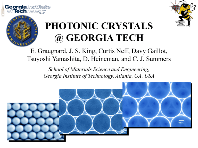
PHOTONIC CRYSTALS
@ GEORGIA TECH
E. Graugnard, J. S. King, Curtis Neff, Davy Gaillot,
Tsuyoshi Yamashita, D. Heineman, and C. J. Summers
School of Materials Science and Engineering,
Georgia Institute of Technology, Atlanta, GA, USA
1D
Photonic Crystals
2D 3D z y x
Periodic in one direction
Periodic in two directions
Periodic in three directions
(Joannopoulos)
• Photonic Crystal – periodic modulation of dielectric constant
• Exhibits a “Photonic Band Gap” (PBG) where propagation of a range of photon energies is forbidden.
• For visible wavelengths, periodicity on order of 150 – 500 nm.
• Introduction of “dielectric defects” yield modes within the PBG.
• Luminescent 2D & 3D PC structures offer the potential for controlling wavelength, efficiency, time response and threshold properties (phosphors, displays, solid state lighting, etc.).
Photonic Crystal Properties
• Density of states of radiation field in free space & photonic crystal
(Sakoda)
• Photonic band gap and associated defect mode are used to create waveguides, microcavities, resonators, couplers and filters.
• Luminescent 2D & 3D PC microcavity structures offer the potential for controlling the wavelength, efficiency, time response and threshold properties by embedding a defect in a photonic crystal structure. (LEDs,
Lasers, Phosphors)
Photonic Crystals:
Dimensionality Defined
• 1-, 2-, & 3-D photonic crystals are all 3-D structures
• Dimensions refer to number of dimensions in which the photonic bandgap exists
• Dielectric constant modulated in 1, 2, or 3 directions.
• Modulation of dielectric constant on the order of the wavelength of illumination source.
Bragg stack
Square lattice of rods
Inverse opal
1D
2D
3D
1-D
2-D
3-D
Real Photonic Crystals:
Applications for thin films
The Bragg Stack:
‘1D Photonic Crystal’ Treatment
• Treat structure with periodicity in order to cast into reciprocal space.
• a = lattice constant
• b = reciprocal lattice constant
• Also, plane waves can be represented by k vector in reciprocal space a
( x )
( x
a ) l b
0 2
/a 4
/a k
2
l
Result of the Bragg Stack
• Dispersion lines: plot of the frequency vs. k vector considering the given structure.
• Similar result to 1-D multiple quantum well problem in solid state physics
• The ‘Photonic Band Gap’ is a range of frequencies where a solution does not exist.
2
a
a w n
w a
2
c w
0
a
2
k a
n
Photonic
Band Gap k
Results Compared:
Photonic Crystal vs. Traditional Optics
• Reflected waves interfere constructively
• Band gap corresponds to high reflectivity
• Thickness of each layer: l layer
4 or l
0 n l layer
= wavelength in medium l
0
= free space wavelength n = refractive index of layer w n
0
a
a
2D Photonic Crystals
Real Space a
Square Lattice r a
Triangular Lattice
Reciprocal Space Band Diagram
X M
G
M K
G
0.6
0.5
0.4
0.3
0.2
0.7
G
0.1
0 G
X M
K M
G
G
2D Photonic Crystals:
Methods of Visualizing Properties
G
M
C
•
Band Surface
– Plot of eigen-solutions in the irreducible
Brillouin zone
– Complete information but difficult to analyze
•
Band Diagram
– Plot of the boundaries of the band surface
– Useful for identifying band gaps and general band shifts
•
Dispersion Curve
– Iso-frequency contours of the band surface
– Useful for identifying refraction and propagation effects
Dispersion Curve Analysis:
Refraction Effects
• The dispersion curve can be used to predict the refraction effects of a photonic crystal.
k
0 n
1
O k
0 n
2
( q
)
Conventional Materials n
1
Interface k
0 n
1 n
2
( q
) k
0 n
2
( q
)
O
Photonic Crystals n
1 n
2
( q
)
Principle of Self-Collimated
Beams
• Conservation of the transverse component of the wave vector
• Group velocity is normal to the dispersion curve
• Possible to achieve nearly parallel beam propagation
4/ w
0
Isotropic Media Photonic Crystal
Nearly Parallel
Beam
2
/a
2D Virtual Waveguides
Beam spreading in an isotropic material
Sharp Turns
Beam spreading in a photonic crystal virtual waveguide
No cross talk
Virtual Waveguide System
Simulation using FDTD
• Photonic band gap perfect mirrors
• Signals can cross with no interference
• Small deviations in beam width and wavelength can be accommodated
1555nm
9.97
m m
1550nm
8.55
m m
1545nm
7.12
m m
2D Superlattice
2D Superlattice
• Based on triangular lattice but with two different hole sizes.
0.5
0.4
0.3
0.2
0.1
M
0
G
M X
X
X’
G
G X’ M
2D Superlattice:
Dispersion Curve
• Large refraction characteristics with small change in incident beam angle
• Effect does not require a band gap
• Effect can be ‘tunable’ by using electro-optic materals
Isofrequency contour
30
20
10
0
-18
-10
-20
-30
-40
-50
-60
-13 -8
Incident Angle
Application: Beam steering/rastering in optical communications or displays
-3
3D Photonic Crystals:
Opals & Inverse Opals
• For 3D PC’s: “top-down” approaches are difficult.
– “Bottom-up” approach: self-assembly
• Most common 3D photonic crystal is the opal.
– Close-packed silica spheres in air
• Opal is used as a template to create an inverse opal.
– Close-packed air spheres in a dielectric material
ALD
3D-PC Opal
26% air
Inverse Opal
74% air for high dielectric contrast
SiO
2
Opal Films
• Opal films are polycrystalline, 10 m m thick, FCC films with the (111) planes oriented parallel to the surface.
• For visible spectrum, lattice constant ~ 140 – 500 nm.
1 µm 300 nm
Challenge: growth of uniform films within a dense, highly porous, high surface-area, FCC matrix
Inverse Opal:
Fabrication
• Self-assembled silica opal template
– 10 μm thick FCC polycrystalline film, (111) oriented.
• Infiltration of opal with high index materials
– ZnS:Mn n~2.5 @ 425 nm (directional PBG)
– TiO
2
(rutile) n avg
~ 3.08 @ 425 nm (omni-directional PBG)
Self
Assembly
Sintered Opal
ALD
Infiltrated Opal
Etch
Inverted Opal
ALD of TiO
2
at 100ºC
(111)
Cross-sections
300 nm
433 nm opal infiltrated with 20 nm of TiO
2
433 nm opal infiltrated with TiO
2
433 nm TiO
2 inverse opal
• TiO
2 infiltration at 100ºC produces very smooth and conformal surface coatings with rms roughness ~2Å.
• Heat treatment (400C, 2 hrs.) of infiltrated opal converts it to anatase TiO
2
, increasing the refractive index from 2.35 to 2.65, with only a 2Å increase in the rms surface roughness.
Optimized TiO
2
Infiltration
• Pulse and purge times were increased to optimize infiltration in opals with small sphere sizes.
2 µm
433 nm TiO
2 inverse opal
Specular Reflectivity
• Measurements: 15° from normal
• Probes changes in G
-L photonic band structure (111)
Flat band peaks
ZnS:Mn
G
-L PPBGs Flat band peaks
TiO
2
G
-L PPBGs
(a) (c) (b)
1.0
0.8
0.6
0.4
(a)
(c)
(b)
0.2
0.0
200 300 400 500 600 700 800
Wavelength (nm)
200 nm opal
400 600 800
Wavelength (nm)
330 nm opal
1000
(a) sintered , (b) as-infiltrated, and (c) inverse opals
Photonic Crystal Properties
• Photonic band diagrams: ω vs. k (reciprocal space representation)
• Calculated from wave form of Maxwell’s equations.
• Plane wave expansion (PWE)
• Finite-difference time domain (FDTD)
Photonic Bands of inverted 3D Si-air PC
U
1.0
0.9
0.8
0.7
0.6
0.5
0.4
0.3
0.2
PPBG
# ixmax= 20
# iymax= 20
# izmax= 20
# dx=1
# ikmax= 16
# n_pts_store=16
# radius=0.5
# eps_b=11.9
# eps_s=1
FCC Brillouin zone
# sig_b=0
• Photonic band gaps (PBG)
• Pseudo-photonic band gaps (PPBG)
Source-->Exec.
metalpc.f90 --> metalpc
• Flat bands, low group velocity project\FDTD\defect\band
• Superprism and giant refraction
0.1
0.0
X U L W K k-vector
Inverse Opal Reflectivity:
Theoretical Comparison
Band Diagram
300
Normalized Reflectivity
Flat band peaks
400
• TiO
2 infiltration of 330 nm opal.
• ~88% filling fraction
• 2.65 Refractive Index
• Agreement: full index attained!
500
600
700
800
900
1000
Fabry-Perot
fringes
2-3 PPBG
1100
L
Sintered Opal
G
700
800
900
400
Normalized Reflectivity
500
600
Flat band
peaks
1000
1100
Band Diagram
2-3 PPBG
L
Infiltrated Opal
G
300
400
500
600
700
800
900
1000
Normalized Intensity
PPBG's
Band Diagram
L Inverse Opal
2-3 PPBG
G
10-11
8-9
5-6
Opal Defect Engineering
Silica Opal with Defect
Infiltrated Opal
Inverted Opal Structure
(With Defect – soon!)
Inverse Opal:
Defect Mode Calculations for PcP
• What is the main idea behind Photonic Crystal Phosphor ?
– Combining a 3D inverse opal with nanophosphors as a local defect in the Pc lattice
40
50
20
30
60
70
10
10 20 30 40 50 60 70
Si-air Pc slice
Luminescent nanocrystal
• Specific frequencies in the Photonic Band-Gap of the inverse structure are inhibited except for the defect modes
• A broad luminescent material spectrum within this band-gap would be filtered by the resonant frequency and therefore tuned up
0.7
0.65
0.6
0.55
0.5
0.45
0.4
0.35
0.3
0
Photonic Band-Gap Analysis
Defect mode
0.5
1 1.5
2
Spectrum analysis for
PcP
Regular spectrum of a green phosphor
Regular spectrum of a defect mode
Both spectrum combine and
Emission Energy of phosphor is totally quenched into the defect mode
Main Characteristics of PcP:
Field of applications
• The cavity mode spectrum lies into the phosphor emission spectrum
– A matching nanophosphor would spontaneously emit in by the confined defect mode in the ultra-high Q-factor cavity
• The nature of the resonant spectrum acts as an optical amplifier and filter and allows Static Tunability of luminescent properties.
– The position and peak cavity spectrum controls the color, luminous intensity and decay time of structure
• Intrinsic properties are therefore controlled by the geometry of the host
• Ultimate tunability would be achieved by optically or electrically biasing materials such as respectively Liquid-crystal or PLZT (instead of air)
– Changing dynamically the refractive index of host materials would affect both position and peak of cavity mode
• The amplified mode leaks upon near-UV pumping and then propagates out
PcPs are perfect candidates for High-Definition Display devices !!!!
Three-Layer Inverse Opal:
PcP
• SEM of TiO
2
/ZnS:Mn/TiO
2 inverse opal
330 nm sphere size
Luminescent multi-layered inverse opals fabricated using ALD: PcP
Photoluminescence:
ZnS:Mn/TiO
2
Composite PcP
• 433 nm opal
• 337 nm N
2 laser excitation
• Detection normal to surface
Cl
-
Mn
2+
(a) 2-layer TiO
2
/ZnS:Mn/air
(14 nm/20 nm) inverse opal
(b-f) 3-layer TiO
2
/ZnS:Mn/TiO
2 inverse opal after backfilling with TiO
2
(b) 1 nm by
(c) 2 nm
(d) 3 nm
(e) 4 nm
(f) 5 nm
108%
(a)
(b)
(c)
(d)
(e)
(f)
400 500 600 700
Wavelength (nm)
800
Using ALD of TiO
2
to create novel 2D Photonic Crystals.
X. D. Wang, E. Graugnard, J. S. King,
C. J. Summers, and Z. L. Wang
TiO
2
Coated ZnO Arrays
Aligned ZnO nano-rods in a hexagonal matrix on a sapphire substrate.
Aligned ZnO nano-rods coated with 100 nm of TiO
2 at 100°C.
Summary
• Precise control of thin film growth enables novel photonic crystal structures:
– Inverse opals with void space air pockets (enhanced PBG)
– Achieved maximum infiltration of 86%
– Perfect match between reflectivity and calculated band structure
– Multi-layered luminescent inverse opals: PcP
• Modification of photoluminescence by precise infiltration
– Increased Mn 2+ peak intensity by 108%
• Pathway for photonic crystal band gap engineering.
• Novel 2D PCs created with ALD
– TiO
2
/ZnO aligned nano-rod arrays
Acknowledgments
• US Army Research Lab: S. Blomquist, E.
Forsythe, D. Morton
• Dr. Won Park, U. Colorado
• Dr. Mike Ciftan, US Army Research Office:
MURI “Intelligent Luminescence for
Communication, Display and
Identification”
