MOSFET - AC Analysis (Common Source and Common Drain)
advertisement
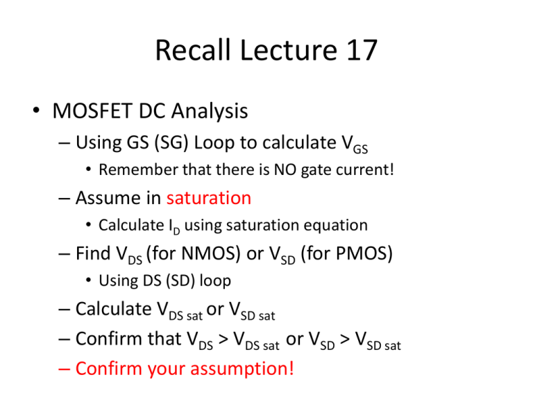
Recall Lecture 17 • MOSFET DC Analysis – Using GS (SG) Loop to calculate VGS • Remember that there is NO gate current! – Assume in saturation • Calculate ID using saturation equation – Find VDS (for NMOS) or VSD (for PMOS) • Using DS (SD) loop – Calculate VDS sat or VSD sat – Confirm that VDS > VDS sat or VSD > VSD sat – Confirm your assumption! APPLICATION OF MOSFETS Digital Logic Gates NOR gate NOR gate response NAND gate The NAND gate response 0 0 High 0 0 High 5 0 Low 5 0 High 0 5 Low 0 5 High 5 5 Low 5 5 Low CHAPTER 7 Basic FET Amplifiers • For linear amplifier function, FET is normally biased in the saturation region. AC PARAMETERS ro = VA / IDQ where VA = 1/ The MOSFET Amplifier - COMMON SOURCE • The output is measured at the drain terminal • The gain is negative value • Three types of common source – source grounded – with source resistor, RS – with bypass capacitor, CS Common Source - Source Grounded ● A Basic Common-Source Configuration: Assume that the transistor is biased in the saturation region by resistors R1 and R2, and the signal frequency is sufficiently large for the coupling capacitor to act essentially as a short circuit. EXAMPLE VDD = 5V The transistor parameters are: VTN = 0.8V, Kn = 0.2mA/V2 and = 0. 520 k Rsi 0.5 k ID = 0.2441 mA gm = 0.442 mA/V 320 k RD = 10 k 0.5 k RTH 198.1 k 0.442 vgs RD = 10 k 1. The output resistance, Rout = RD 2. The output voltage: vo = - gmvgs (Rout) = - gmvgs (10) = -4.42 vgs 3. The gate-to-source voltage: vgs = [198.1 / (198.1 + 0.5 )] = 0.9975 vi (replace into equation from step 2) 4. So the small-signal voltage gain: Av = vo / vi = - 4.41 , Ri = RTH Type 2: With Source Resistor, RS VTN = 1V, Kn = 1.0mA / V Perform DC analysis Assume transistor in saturation VG = ( 200 / 300 ) x 3 = 2 V Hence, KVL at GS Loop: VGS + IDRS – VTH = 0 VGS = 2 – 3ID KVL at DS loop VDS + 10 ID + 3ID – 3 = 0 VDS = 3 -13 ID Assume biased in saturation mode: Hence, ID = 1.0 (2 – 3ID - 1 )2 = 1.0 (1 – 3ID )2 9 ID2 – 7 ID + 1 = 0 VTN = 1V, Kn = 1.0 mA / V ID = 0.589 mA VGS = 2 – 3ID = 0.233 < VTN MOSFET is OFF Not OK ID = 0.19 mA VGS = 2 – 3ID = 1.43 V > VTN OK VDS = 3 -13 ID = 0.53 V VDS sat = VGS - VTN = 1.43 – 1.0 = 0.43 V 0.53 V > 0.43 V Transistor in saturation Assumption is correct! + V’ RTH 66.67 k RD = 10 k RS = 3 k - 1. The output voltage: gm = 0.872 mA/V vo = - gmvgsRD = - 0.872 ( vgs) (10) = - 8.72 vgs 2. Find v’ v’ = vgs + gmvgs RS v’ = vgs(1 + 2.616) = 3.616 vgs + V’ RTH 66.67 k RD = 10 k RS = 3 k - 3. Find v’ in terms of vi : using voltage divider v’ = [RTH / (Rsi + RTH)] vi But in this circuit, Rsi = 0 so, v’ = vi = 3.616 vgs 4. Go back to vo equation: vo = - 8.72 vgs vo = - 8.72 ( vi / 3.616) AV= vo / vi = - 2.41 Type 3: With Source Bypass Capacitor, CS Circuit with Source Bypass Capacitor ● An source bypass capacitor can be used to effectively create a short circuit path during ac analysis hence avoiding the effect RS ● CS becomes a short circuit path – bypass RS; hence similar to Type 1 IQ = 0.5 mA hence, ID = 0.5 mA gm = 2 Kn ID = 1.414 mA/V ro = RG 200 k 1.414 vgs RD = 7 k 1. The output voltage: vo = - gmvgs (RD) = -1.414 (7) vgs = - 9.898 vgs 2. The gate-to-source voltage: vgs = vi in parallel ( no need voltage divider) So the small-signal voltage gain: Av = vo / vi = - 9.898 The MOSFET Amplifier - COMMON DRAIN • The output is measured at the source terminal • The gain is positive value 0.5 k 0.5 k 150 k 113.71 RTH k 470 k 0.75 k ID = 8 mA , Kn = 4 mA /V2 gm = 2 Kn ID = 11.3 mA/V gm = 2 Kn ID = 11.3 mA/V + v’ - 1. The output resistance, Rout = ro || Rs 2. The output voltage v = g v (r R ) = 11.3 v (0.70755) = 8 v o m gs o S gs gs 3. v’ in terms of vi: v’ = (RTH / RTH + RSi) vi = 0.9956 vi 4. KVL at supermesh: vgs + gmvgs (ro RS) – v’ = 0 v’ = vgs + 8 vgs vgs = v’ / [1+8] = 0.9956 vi / 9 = 0.111 vi (replace into equation from step 2) 5. The voltage gain Av = vo / vi = 0.8875

