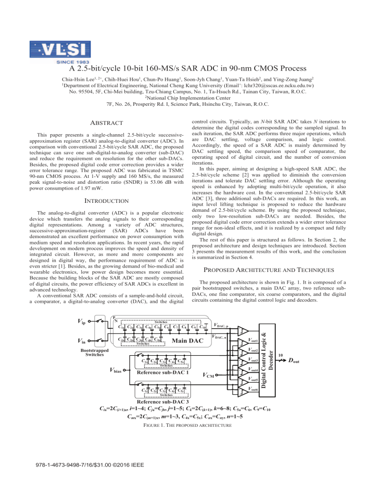
A 2.5-bit/cycle 10-bit 160-MS/s SAR ADC in 90-nm CMOS Process Chia-Hsin Lee1, 2+, Chih-Huei Hou1, Chun-Po Huang1, Soon-Jyh Chang1, Yuan-Ta Hsieh2, and Ying-Zong Juang2 Department of Electrical Engineering, National Cheng Kung University (Email+: lchr320@sscas.ee.ncku.edu.tw) No. 95504, 5F, Chi-Mei building, Tzu-Chiang Campus, No. 1, Ta-Hsuch Rd., Tainan City, Taiwan, R.O.C. 2National Chip Implementation Center 7F, No. 26, Prosperity Rd. I, Science Park, Hsinchu City, Taiwan, R.O.C. 1 This paper presents a single-channel 2.5-bit/cycle successiveapproximation register (SAR) analog-to-digital converter (ADC). In comparison with conventional 2.5-bit/cycle SAR ADC, the proposed technique can save one sub-digital-to-analog converter (sub-DAC) and reduce the requirement on resolution for the other sub-DACs. Besides, the proposed digital code error correction provides a wider error tolerance range. The proposed ADC was fabricated in TSMC 90-nm CMOS process. At 1-V supply and 160 MS/s, the measured peak signal-to-noise and distortion ratio (SNDR) is 53.06 dB with power consumption of 1.97 mW. INTRODUCTION The analog-to-digital converter (ADC) is a popular electronic device which transfers the analog signals to their corresponding digital representations. Among a variety of ADC structures, successive-approximation-register (SAR) ADCs have been demonstrated an excellent performance on power consumption with medium speed and resolution applications. In recent years, the rapid development on modern process improves the speed and density of integrated circuit. However, as more and more components are designed in digital way, the performance requirement of ADC is even stricter [1]. Besides, as the growing demand of bio-medical and wearable electronics, low power design becomes more essential. Because the building blocks of the SAR ADC are mostly composed of digital circuits, the power efficiency of SAR ADCs is excellent in advanced technology. A conventional SAR ADC consists of a sample-and-hold circuit, a comparator, a digital-to-analog converter (DAC), and the digital P N Vip PROPOSED ARCHITECTURE AND TECHNIQUES The proposed architecture is shown in Fig. 1. It is composed of a pair bootstrapped switches, a main DAC array, two reference subDACs, one fine comparator, six coarse comparators, and the digital circuits containing the digital control logic and decoders. Switches C1a C2a C3a C4a C5a C6 C7 C8 C1b C2b C3b C4b C5b Vin control circuits. Typically, an N-bit SAR ADC takes N iterations to determine the digital codes corresponding to the sampled signal. In each iteration, the SAR ADC performs three major operations, which are DAC settling, voltage comparison, and logic control. Accordingly, the speed of a SAR ADC is mainly determined by DAC settling speed, the comparison speed of comparator, the operating speed of digital circuit, and the number of conversion iterations. In this paper, aiming at designing a high-speed SAR ADC, the 2.5-bit/cycle scheme [2] was applied to diminish the conversion iterations and tolerate DAC settling error. Although the operating speed is enhanced by adopting multi-bit/cycle operation, it also increases the hardware cost. In the conventional 2.5-bit/cycle SAR ADC [3], three additional sub-DACs are required. In this work, an input level lifting technique is proposed to reduce the hardware demand of 2.5-bit/cycle scheme. By using the proposed technique, only two low-resolution sub-DACs are needed. Besides, the proposed digital code error correction extends a wider error tolerance range for non-ideal effects, and it is realized by a compact and fully digital design. The rest of this paper is structured as follows. In Section 2, the proposed architecture and design techniques are introduced. Section 3 presents the measurement results of this work, and the conclusion is summarized in Section 4. Switches C9 C10 Main DAC VDAC, p VDAC, n + − + − + Bootstrapped Switches − C1x C2x C3x C4x C5x Vbias + − Switches Reference sub-DAC 1 VCM + − + − C1y C2y C3y C4y C5y Switches + Vout1 Vout2 Vout3 Vout4 Vout5 Vout6 Digital Control Logic & Decoder ABSTRACT − Reference sub-DAC 3 Cia=2C(i+1)a, i=1~4; Cja=Cjb, j=1~5; Ck=2C(k+1), k=6~8; C5a=C6, C9=C10 Cmx=2C(m+1)x, m=1~3, C4x=C5x; Cnx=Cny, n=1~5 FIGURE 1. THE PROPOSED ARCHITECTURE 978-1-4673-9498-7/16/$31.00 ©2016 IEEE 10 Dout In the first two bit-conversion cycles, six coarse comparators compare the voltages on the top plates of main DAC (VDAC) with the threshold voltages (Vr) for 2.5-bit/cycle scheme. Then one fine comparator is used for 1-bit/cycle operation in the remaining cycles. The ADC speed will be faster if more iterations are executed by 2.5bit/cycle scheme. (i.e., fewer 1-bit/cycle operations.) However, the mismatch between the coarse and fine comparators results in a dynamic offset error. Since the tolerance range is smaller in latter iterations, it may not be tolerated by digital code error correction and thus degrade the ADC linearity. Therefore, the 2.5-bit/cycle operation is performed only two cycles to improve the operation speed without compromising the ADC linearity. The 2.5-bit/cycle scheme in SAR architecture is similar to the operation of sub-ADC in a 2.5-bit/stage pipelined ADC, except for the variable Vr in each cycle. In conventional 2.5-bit/cycle scheme, the reference voltage (Vref) can be divided into seven regions by six Vr in each cycle. For instance, 3/16, 5/16, 7/16, 9/16, 11/16, and 13/16 of Vref can be chosen as the six Vr in the 1st cycle, as shown in Fig. 2. By comparing VDAC with Vr, the region where VDAC locate can be found, and the specific capacitors switch according to the located region. For example, if VDAC locate in region B, the most significant bit (MSB) capacitor switches in this cycle. Input Level Lifting Technique The proposed input level lifting technique is implemented in 2.5bit/cycle scheme. The concept of this technique is to generate one Vr by shifting VDAC up. As a result, one of Vr can be easily generated without sub-DAC. The detail operation of the proposed technique is shown in Fig. 3. In the beginning of the 1st cycle, VDAC are shifted up with Vref/16 (denoted by Vs1). Then the difference between VDAC and VCM (=Vref/2) now becomes VDAC為Vref/16炼VCM which is equal to VDAC 炼7Vref/16. Thus, the Vr of 7Vref/16 can be replaced by VCM. In this case, because VDAC locate in region D, VDAC remain unchanged. Therefore, it is unnecessary to switch any capacitors. After the 1st cycle, the similar operation is executed in the 2nd cycle. By shifting Vref Switch Both (Region A) 13 VCM Vref Switch MSB (Region B) 16 Switch MSB-1 (Region C) 16 No Switching (Region D) 16 Switch MSB-1 (Region C) 16 Switch MSB (Region B) 16 11 Vref 9 7 5 3 Vref Vref Vref Vref 16 Switch Both (Region A) 0 FIGURE 2. THE SEVEN REGIONS IN THE CONVENTIONAL 2.5-BIT/CYCLE SCHEME 1st Cycle Vref +Vs1 2nd Cycle 5 A 8 Vref A B B C C −Vs1+Vs2 1 −Vs2 − Vref 64 D D C C B B A A 3 0 8 1 −Vs2 + Vref ( = 0 ) 64 Vref VDAC Vr VCM FIGURE 3. THE PROPOSED INPUT LEVEL LIFTING TECHNIQUE VDAC up with Vref/64 (denoted by Vs2), the Vr of 31Vref/64 can be replaced by VCM. Meanwhile, the shifted voltage Vs1 in the first cycle should be recovered. This “recover” function has to be executed in the beginning of the next cycle to guarantee a correct signal for comparing. In this case, VDAC locate in region C after Vs1 and Vs2 being settled. Thus, the MSB-3 capacitor (C4) are switched, and VDAC is switched by Vref/64. After the 2nd cycle finished, the second raised voltage Vs2 is taken back in the 3rd cycle and the overall conversion is proceeded in 1-bit/cycle operation after then. The “shifting” behavior is implemented by switching the capacitors in main DAC. In the 1st cycle, Vs1 is generated by pulling C3b up in Fig. 1. The similar operation is executed in the 2nd cycle by pulling C5b up, and Vs1 is recovered by pulling C3b down. Since both VDAC and Vr are differential, the six Vr can be simplified to three single-ended signals with single-ended comparison [4]. By using the proposed technique, the original Vr (7/16, 11/16, 13/16 of Vref in the 1st cycle and 27/64, 31/64, 35/64 of Vref in the 2nd cycle) are shifted to 1/2, 3/4, 7/8 of Vref and 7/16, 1/2, 9/16 of Vref in the 1st and 2nd cycle, respectively. Consequently, the resolution requirement of the sub-DACs to generate the Vr mentioned above is reduced to only four bits. The overall operation procedure is shown in Fig. 4. In order to simplify the digital circuits of the 2.5-bit/cycle scheme, the commonmode voltage between VDAC, p and VDAC, n is restricted to VCM. Thus, the first four capacitors (C1~C4) are switched by the split-monotonic switching method [5]. In addition, the fifth capacitors (C5) is also switched by the same method to implement the proposed technique. The remaining capacitors (C6~C9) are switched by the monotonic switching method [6]. Comparing with the work which employs conventional 2.5bit/cycle operation [3], one sub-DAC is omitted with the proposed input level lifting technique. Furthermore, the required resolution of sub-DAC is reduced from 6 bits to 4 bits. Digital Code Error Correction In proposed 2.5-bit/cycle structure, the total capacitance of main DAC and that of sub-DACs are unequal. Therefore, an error (Verror) between the inputs of coarse comparator is induced by non-ideal effects such as gain error, kickback noise, and non-ideality of S/H circuit, as shown in Fig. 5. This error degrades the performance especially in single-ended structure. State Sample Conversion Cycle 1 Cycle 2 Cycle 3 Cycle 4 Cycle 5 Cycle 6 Cycle 7 Cycle 8 Operation scheme 2.5-bit/cycle Switching Reset/ Split-monotonic switching method Sample Switched C1, C2 C3, C4 capacitor in C5 (C3b*) (C5b*) main DAC 1-bit/cycle Monotonic switching C6 C7 C8 C9 *The capacitors for shifted voltage (Vs1 and Vs2) FIGURE 4. THE CIRCUIT OPERATION PROCEDURE Switches + Ctotal(main DAC) 5 Vref 8 Verror + FIGURE 5. THE ERROR OF NON-IDEAL EFFECTS VDAC, n Switches Coarse Comparator B C D T X X X X X X X T X X X X X X X T X X X X X X X T X X X X X X X T X X X X X X X T X X X X X X X T D Ctotal(sub-DAC) A 1 Vref 2 C B 3 Vref 8 A 5 Vref 8 1 Vref 2 VDAC, p FIGURE 6. IDEAL TRUTH TABLE 5 Vref 8 A B C D T X X X X X X ET T X X X X X F ET T X X X X F ET ET T X X X D VDAC, n + Verror As mentioned before, there is an error tolerance range when 2.5bit/cycle scheme is applied. In the 1st cycle, the magnitude of the error tolerance range is Vref/16, while the magnitude in the 2nd cycle is shrunk to Vref/64. This tolerance range may not be sufficient if various errors such as comparators offset error, capacitor mismatch, and Verror mentioned above happen simultaneously. Thus, a digital code error correction is proposed to extend the error tolerance range in the 2nd cycle. Besides, the extended error tolerance range can enhance the ADC performance with low cost. The truth table in Fig. 6 shows the ideal conversion of the differential input signals, VDACp and VDACn, to the comparison results (denoted as A to D) in one cycle of 2.5-bit/cycle operation. The lines between the comparison results represent the threshold voltages mentioned in Section 2.1. “T” marked in the table means the 7 output results in 2.5-bit/cycle operation and “X” denotes the “don’t care” situation with ideal signals of VDAC. Figure 7 shows the real situation when negative offset occurs. In this table, both “ET” and “F” imply wrong outputs. “ET” means the situation tolerated by 2.5-bit/cycle scheme, whereas “F” means the wrong codes that is out of tolerance. To solve the problem, the proposed digital code error correction matches up the wrong codes with the correct ones. As the example shown in Fig. 7, the correct output circled is CC. When the magnitude of error increases and leads to the “F” region, the output becomes BB. By adding a correction table behind the outputs of coarse comparators, the proposed technique corrects the output results from BB to CC. With the correction scheme, the maximum error tolerance range in the 2nd cycle is increased from Vref /64 to 5Vref /64 (i.e., 5 times wider). Instead of trying to directly alleviate the non-ideal effects, this technique is accomplished more easily in digital way without a complicated analog design. 1 Vref 2 C X F F ET T X X X F F ET ET T X X X X T B 3 Vref 8 F F ET 1 Vref 2 VDAC, p + Verror FIGURE 7. NON-IDEAL TRUTH TABLE A 5 Vref 8 TABLE I. COMPARISON WITH STATE-OF-THE-ART WORKS Specifications [7] [8] [9] This Work Architecture 1b 1.5b 2b 2.5b Technology (nm) 40 65 65 90 Supply (V) 0.9 1.2 1 1 Resolution (bit) 10 10 8 10 Sampling Rate (MS/s) 200 160 250 160 ENOB (bit) 9.20 8.96 7.47 8.52 Power (mW) 0.818 3.4 1.8 1.97 FoM (fJ/conv.-step) 13.9 43 42 33.5 Active Area (mm2) 0.013 0.015 0.024 0.11 MEASUREMENT RESULTS The proposed ADC was fabricated in TSMC 1P9M 90-nm CMOS process. The micrograph of the ADC is shown in Fig. 8. The measured DNL and INL are shown in Fig. 9. The peak DNL and INL are +1.19/-0.91 LSB and +2.21/-1.28 LSB, respectively. At 160 MS/s, 1-V supply and 10 MHz input frequency, the SNDR and SFDR are 53.06 and 70.03 dB, respectively. The resultant ENOB is 8.52 bits. Fig. 10 shows the measured FFT spectrum with a 1/16 frequency division. The total power consumption is 1.97 mW. The FoM of the ADC is 33.5 fJ/conversion-step. Table I summarizes the comparison with other state-of-the-art ADCs. CONCLUSION S/H Digital Control Logic Comparator Sub-DAC Main DAC 420 m Main DAC Comparator In this paper, we proposed an input level lifting technique to reduce the hardware demand of 2.5-bit/cycle scheme. In addition to the omission of one sub-DAC, the resolution requirement of the other sub-DACs is also decreased from 6 bits to 4 bits. The proposed digital code error correction extends 5 times error tolerance range of 2.5-bit/cycle scheme by a compact and fully digital design. The prototype achieves 160 MS/s operational speed with a FoM of 33.5 fJ/conversion-step at 1-V supply voltage. Decoder 262.8 m ACKNOWLEDGEMENT Divider & Output Buffer FIGURE 8. DIE PHOTO AND DETAIL LAYOUT VIEW The authors would like to thank the fabrication and measurement support of Chip Implementation Center (CIC), Taiwan. This work was supported in part by the grant of MOST 104-2220-E-006-012from Ministry of Science and Technology, Taiwan. REFERENCES [1] [2] [3] [4] FIGURE 9. MEASURED DNL AND INL [5] [6] [7] [8] [9] FIGURE 10. MEASURED FFT SPECTRUM AT 160 MS/S D. Robertson, “The past, present, and future of data converters and mixed signal ICs: a universal model,” in IEEE Symp. VLSI Circuits Dig. Tech. Papers, Jun. 2006, pp. 1–4. D. W. Cline, and P. R. Gray, “A power optimized 13-b 5 Msamples/s pipelined analog-to-digital converter in 1.2 μm CMOS,” IEEE J. Solid-State Circuits, vol. 31, no. 3, pp. 294– 303, Mar. 1996. N.-Y. Wang, “A 10-bit 110-MS/s SAR ADC with 2.5-bit predictive capacitor switching procedure,” M.S. thesis, Dept. Elect. Eng., National Cheng Kung Univ., Tainan, Taiwan, 2011. G.-Y. Huang et al., “1-uW 10-bit 200-kS/s SAR ADC with a bypass window for biomedical applications,” IEEE J. SolidState Circuits, vol.47, no.11, pp.2783–2795, Nov. 2012. C.-C. Liu et al., “A 1V 11fJ/Conversion-Step 10bit 10MS/s asynchronous SAR ADC in 0.18m CMOS,” in IEEE Symp. VLSI Circuits Dig. Tech. Papers, Jun. 2010, pp. 241–242. C.-C. Liu et al., “A 10-bit 50-MS/s SAR ADC with a monotonic capacitor switching procedure,” IEEE J. Solid-State Circuits, vol. 45, no. 4, pp. 731–740, Apr. 2010. G.-Y. Huang et al., “A 10b 200MS/s 0.82mW SAR ADC in 40nm CMOS,” in IEEE A-SSCC, Nov. 2013, pp. 289–292. R. Vitek et al., “A 0.015mm2 63fJ/conversion-step 10-bit 220MS/s SAR ADC with 1.5b/step redundancy and digital metastability correction,” in Proc. IEEE CICC, Sept. 2012, pp. 1–4. H. Wei et al., “A 0.024mm2 8b 400MS/s SAR ADC with 2b/cycle and resistive DAC in 65nm CMOS,” in IEEE ISSCC Dig. Tech. Papers, Feb. 2011, pp. 188–190.


