2017 Progress In Electromagnetics Research Symposium — Spring (PIERS), St Petersburg, Russia, 22–25 May
New Electrical Equivalent Circuit Model of the Inset Fed
Rectangular Patch Antenna
Wissem Chouchene, Chiraz Larbi, and Taoufik Aguili
Communications Systems Laboratory (SysCom), National Engineering School of Tunis (ENIT)
University of Tunis El Manar (UTM), Tunisia
Abstract— We present through the study of the discontinuity between transmission line and
conductor backed coplanar wave guide a new accurate equivalent circuit model for the inset fed
rectangular patch antenna. In this work the inset fed rectangular patch antenna is decomposed
into three parts: transmission line part which is the feed line. The second part is the conductor
backed coplanar waveguide witch is at the middle of the antenna structure, and the last one,
is again, a transmission line one. Each of these parts will be studied a part: each of them
is characterized by its characteristic impedance Zc and its electrical length β computed via
LineCalc tool of Advanced design system software than all parts will be put together to form
our antenna, but we have to study the discontinuities impact. In order to provide a perfect
electrical model of the antenna at the resonance frequency the parameters for each discontinuity
are computed using the reflection parameter: S11 and transmission parameter: S12 related to the
brought backed impedance for each part of the antenna. the validation of this work is done by
the Momentum solver of Advanced Design System environment software, by taking into account
the studied discontinuities and simulating the electrical circuit model on the same software so
the comparison between S11 given by the circuit model simulation and the one given by the
electromagnetic Momentum simulation show a great accordance around the resonance frequency.
Such electrical circuit model is very useful in front end simulation and it show the importance of
the discontinuities which are neglected for most electrical model.
1. INTRODUCTION
Having an accurate electrical equivalent circuit model of a rectangular patch antenna is the subject
of many communications [1, 2] and CAD engineering application [3]. Most proposed models are
based essentially on a simple transmission line model or resonant cavity model [4].
In this work, we focus on the equivalent circuit of an inset fed rectangular patch antenna,
using in addition to the transmission line model a conductor backed coplanar wave guide model
beside the study of the electromagnetic behavior for each discontinuity,so that the electrical model
became more accurate. We used the Momentum and ADS environment for both electromagnetic
and electrical stimulation. The tow simulations of the S11 (dB) results are compared to validate
the model accuracy around the resonant frequency.
2. THE CONVENTIONAL MODEL
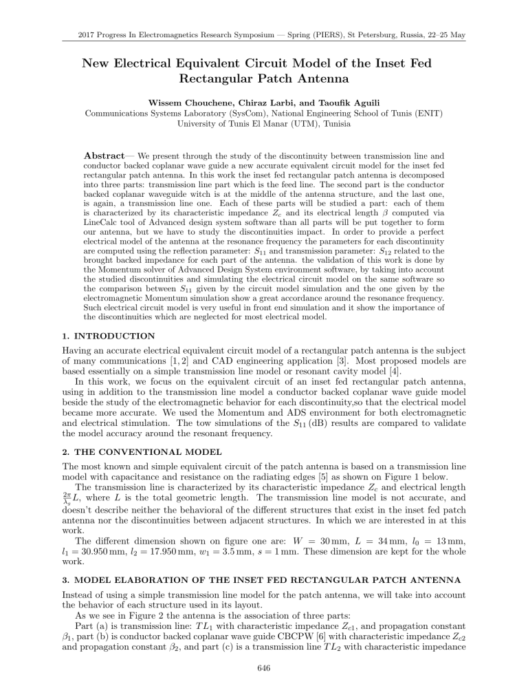
The most known and simple equivalent circuit of the patch antenna is based on a transmission line
model with capacitance and resistance on the radiating edges [5] as shown on Figure 1 below.
The transmission line is characterized by its characteristic impedance Zc and electrical length
2π
λg L, where L is the total geometric length. The transmission line model is not accurate, and
doesn’t describe neither the behavioral of the different structures that exist in the inset fed patch
antenna nor the discontinuities between adjacent structures. In which we are interested in at this
work.
The different dimension shown on figure one are: W = 30 mm, L = 34 mm, l0 = 13 mm,
l1 = 30.950 mm, l2 = 17.950 mm, w1 = 3.5 mm, s = 1 mm. These dimension are kept for the whole
work.
3. MODEL ELABORATION OF THE INSET FED RECTANGULAR PATCH ANTENNA
Instead of using a simple transmission line model for the patch antenna, we will take into account
the behavior of each structure used in its layout.
As we see in Figure 2 the antenna is the association of three parts:
Part (a) is transmission line: T L1 with characteristic impedance Zc1 , and propagation constant
β1 , part (b) is conductor backed coplanar wave guide CBCPW [6] with characteristic impedance Zc2
and propagation constant β2 , and part (c) is a transmission line T L2 with characteristic impedance
646
2017 Progress In Electromagnetics Research Symposium — Spring (PIERS), St Petersburg, Russia, 22–25 May
(a)
(b)
(c)
(c)
(a)
(b)
Figure 1: Patch antenna equivalent circuit based on
transmission line model.
Figure 2: Inset fed rectangular patch antenna structures.
Zc3 , and propagation constant β3 . When associating these three parts in series as in the layout of
the patch antenna we obtain a new equivalent circuit of the patch antenna as shown on Figure 3.
Figure 4: S11 (dB).
Figure 3: Equivalent circuit based on transmission
lines and CBCPW.
The comparison of dB (S11 ) parameter for both circuit simulation and electromagnetic is shown
on Figure 4.
As we see on Figure 4 above, the tow simulations are discordant expect at the resonant frequency,
the bandwidth for the equivalent circuit is too large comparing to the reel bandwidth of the antenna.
So such equivalent circuit can only be used at the frequency resonance of the patch which is a
singular frequency point and not practical for CAD engineering. In order to make the equivalent
circuit valid on large interval of frequency we introduce the study of discontinuities.
4. DISCONTINUITIES STUDY
We improve the previous circuit by modeling the discontinuities between the Transmission line T L1
and the conductor backed coplanar wave guide CBCPW in first step and between the CBCPW
and transmission line 2: T L2 in second step. These tow discontinuities: D1 and D2 are shown on
Figure 5 and will be studied using the chain matrix.
647
2017 Progress In Electromagnetics Research Symposium — Spring (PIERS), St Petersburg, Russia, 22–25 May
Figure 5: D1 and D2 discontinuities between adjacent parts of the rectangular patch antenna.
Figure 6: Discontinuity D1 in the equivalent circuit
of the antenna and chain matrix disposition.
4.1. Adding the D1 Discontinuity Model
To calculate the equivalent circuit model of the discontinuity D1 we use the chain matrix for each
part of the antenna structure we denote: [C1 ] the chain matrix for transmission line T L1 , [D1 ] is
the chain matrix for the discontinuity D1 , [C2 ] is the chain matrix for the CBCPW and [C3 ] is the
chain matrix for transmission line T L2 . All these matrixes are put in chain as shown on Figure 6
the whole chain matrix of the antenna is denoted [CT ].
We chose a T form for the D1 discontinuity as seen on Figure 7 bellow.
Figure 7: T form of the discontinuity D1 .
Figure 8: Patch antenna equivalent circuit with discontinuity D1 .
Each chain matrix is expressed in function of Sij parameters. For each part of the antenna a 2
ports simulation is done by Momentum. [D1 ] is our unknown discontinuity matrix:
[CT ] = [C1 ] [D1 ] [C2 ] [C3 ] → [D1 ] = [C1 ]−1 [CT ] [C3 ]−1 [C2 ]−1
The relation between each impedance
Z1 , Z2 and Z3 , in the discontinuity [D1 ] in Figure 7 and the
A B
are:
elements of the matrix [D1 ] =
C D
A=
Z1 + Z3
,
Z3
B=
Z2 (Z2 + Z3 )
,
Z1
C=
1
,
Z1 + Z3
D=−
(Z2 + Z3 )
Z3
So we can deduce the nature and the value for each impedance of the discontinuity:
Z1 = jωL1 → L1 = 10 pH
Z2 = jωL2 → L2 = 15 pH
1
Z3−1 =
+ jωC → R = 45 Ohm and C = 24 pF
R
Including the D1 discontinuity model into the patch equivalent circuit of the Figure 3, the improved
equivalent circuit is shown on Figure 8.
The comparison between the S11 (dB) parameter is shown on Figure 9.
648
2017 Progress In Electromagnetics Research Symposium — Spring (PIERS), St Petersburg, Russia, 22–25 May
Figure 9: S11 (dB).
Figure 10: Chain matrix in correspondence with the
different parts of the antenna.
Comparing to the previous simulation, Figure 4, there is a visible improvement of the S11 (dB)
parameter when considering the D1 discontinuity, but the bandwidth of the equivalent circuit is
larger than the real one of the electromagnetic simulation.
In order to obtain more coincidence of S11 (dB) parameter we will consider, in the next paragraph, both D1 and D2 discontinuities.
4.2. Adding the D1 and D2 Discontinuities Models
In this part we take into account the tow discontinuities D1 and D2 as shown on Figure 10. The
electrical model for each discontinuity is deduced from its chain matrix, respectively [D1 ], [D2 ].
To obtain the matrix: [D1 ] and [D2 ] we use the chain matrix concept: in one hand the total
chain matrix for the whole antenna and in the other hand the matrix for each part of the antenna,
adding the discontinuity matrix Figure 10.
The global equation of chain matrix for the whole antenna including the discontinuity D1 and
D2 is:
(1)
[CT ] = [C1 ] [D1 ] [C2 ] [D2 ] [C3 ]
To solve the Equation (1) in [D1 ] and [D2 ] we consider tow frequency points around the resonant
frequency of the inset fed rectangular patch antenna denoted f1 and f2 :
[CT ]|f1 = [C1 ]|f1 [D1 ] [C2 ]|f1 [D2 ] [C3 ]|f1
(2)
[CT ]|f2 = [C1 ]|f2 [D1 ] [C2 ]|f2 [D2 ] [C3 ]|f2
where [CT ]|fk , k = {1, 2} is the total chain matrix of the patch at frequency fk , and which is a
function of scattering parameters matrix: [CT ]|fk = [f (Sij|fk )]. From (2) we deduce the value for
each discontinuity matrix [D1 ] and [D2 ] we chose a ‘T ’ form for both discontinuities, as shown on
Figure 11.
(i)
(i)
(i)
A(i) B (i)
V2
V1
V2
= [Di ]
=
(i)
(i)
(i)
C (i) D(i)
I1
−I2
−I2
(a)
(b)
Figure 11: ‘T ’ form for the discontinuity i = {1, 2}.
Figure 12: Discontinuities equivalent electrical circuit (a) for D1 , (b) for D2 .
649
2017 Progress In Electromagnetics Research Symposium — Spring (PIERS), St Petersburg, Russia, 22–25 May
where i represent the discontinuity 1 or 2
A(i) =
(i)
Z1
+
Z3i
(i)
Z3
,
C (i) =
(i)
1
(i)
Z1
+
(i)
Z3
,
B (i) =
Z2
(i)
(i)
Z2 + Z3
(i)
Z1
and D(i) = −
(i)
(i)
Z2 + Z3
(i)
Z3
From each discontinuity matrix [Di ] i = {1, 2} computed previously we deduce the impedances
types and values as seen on Figure 12.
Where R1 = 1.4 Ohm, R2 = 3.9 Ohm, L1 = 9.38 nH, L2 = 3.5 nH, C = 0.0111 pF, R =
1790 Ohm, R3 = 0.9 Ohm, R4 = 0.8 Ohm, C1 = 0.01 pF.
So the equivalent electrical circuit of the inset fed rectangular patch antenna including discontinuities models is shown below on Figure 13.
Figure 14: S11 (dB).
Figure 13: Improved equivalent electrical circuit of
the inset fed rectangular patch antenna.
Comparing to the previous model a significant improvement of the S11 (dB) parameter is observed on Figure 14. In fact the dB (S11 ) parameter of the equivalent circuit of the patch antenna
is nearly the same as that of the electromagnetic simulation. So the equivalent circuit is valid on
large frequency interval and not only a singular coincidence as in Figure 4.
5. CONCLUSION
In this study we have improved in many steps the equivalent electrical circuit of the inset fed
rectangular patch antenna by studying discontinuities existing on its structure. First, instead of
using only the transmission line model, we have added CBCPW model, and then we take into
account the discontinuities between the different structures to obtain finally new electrical circuit
model for the inset fed rectangular patch antenna that shows a great accordance for the S11 (dB) of
the electromagnetic simulation and the electrical simulation. However, to be useful by microwave
engineering, a formulation for the different electrical parameters of the equivalent electrical model
of the inset fed rectangular path antenna in function of geometrical parameters is needed.
REFERENCES
1. Pues, H. and A. van de Capelle, “Accurate transmission-line model for the rectangular microstrip antenna,” IEE Proceedings H — Microwaves, Optics and Antennas, Vol. 131, No. 6,
Dec. 1984.
2. Hafiane, A., L. Cirio, and O. Picon, “Electrical model and mutual coupling between microstrip
antennas expressed through FDTD method,” IEEE Microwave Conference, Oct. 2000.
3. Kapsidis, D., M. T. Chryssomallis, and C. G. Christodoulo, “An accurate circuit model of a
microstrip patch antenna for CAD applications,” Antennas and Propagation Society International Symposium, IEEE Conference Publcations, Jun. 2003.
4. Sainati, R. A., “Microstrip radiator models,” CAD of Microstrip Antennas for Wireless Applications, 29–41, Artech House, 1996.
5. Kumar, G. and K. P. Ray, Regularly Shaped Broadband MSAs in Broadband Microstrip Antennas, 30–114, Artech House, 2003.
650
2017 Progress In Electromagnetics Research Symposium — Spring (PIERS), St Petersburg, Russia, 22–25 May
6. Simons, R. N., “Conductor-backed Coplanar Waveguide” in Coplanar Waveguide Circuits,
Components, and Systems, 87–90, John Wiley & Sons, 2001.
651
