A Bootstrap Voltage Clamping Circuit for Dynamic VTH Characterization in Schottky-Type p-GaN Gate Power HEMT
advertisement
The 33rd International Symposium on
Power Semiconductor Devices and ICs (ISPSD)
May 30 - June 3, 2021, Nagoya Full Virtual Conference
2-2
A Bootstrap Voltage Clamping Circuit for Dynamic
VTH Characterization in Schottky-Type p-GaN Gate
Power HEMT
Kailun Zhong, Han Xu, Song Yang, Zheyang Zheng, Junting Chen, and Kevin J. Chen
Department of Electronic and Computer Engineering, The Hong Kong University of Science and Technology, Hong Kong
Phone: +852-23588530, Email: kzhongac@connect.ust.hk, eekjchen@ust.hk.
G
p-GaN
S
G
Passivation
D
AlGaN
GaN
Transition layer
Si substrate
2DEG
p-GaN
AlGaN
DSch
Dpin
GaN
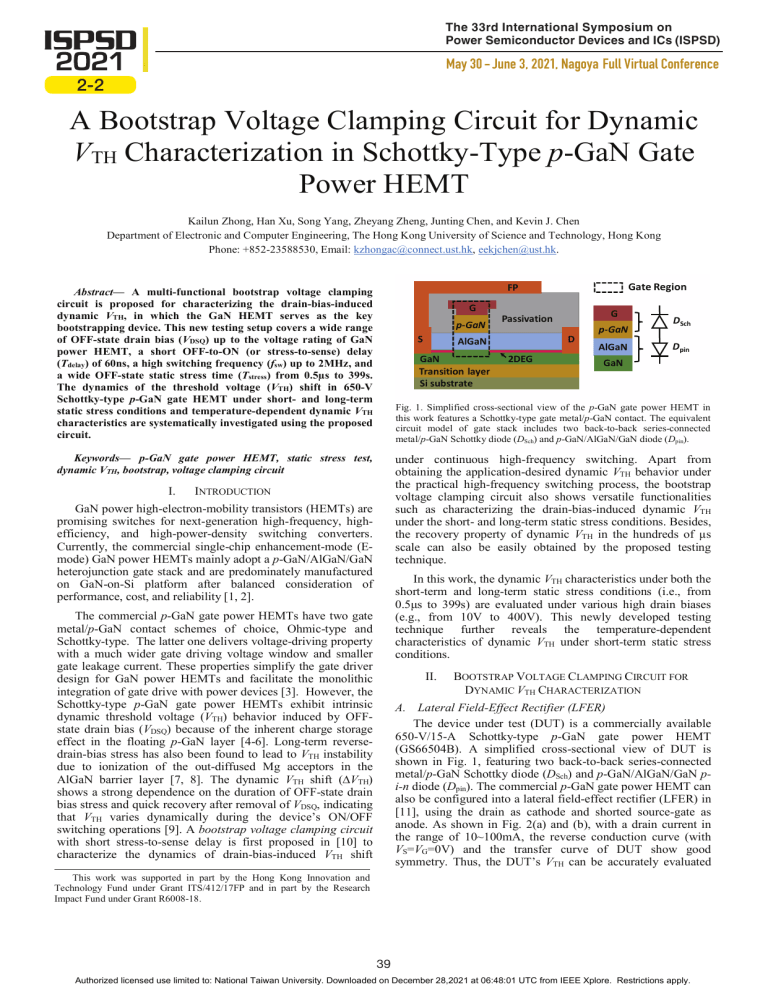
Fig. 1. Simplified cross-sectional view of the p-GaN gate power HEMT in
this work features a Schottky-type gate metal/p-GaN contact. The equivalent
circuit model of gate stack includes two back-to-back series-connected
metal/p-GaN Schottky diode (DSch) and p-GaN/AlGaN/GaN diode (Dpin).
Keywords— p-GaN gate power HEMT, static stress test,
dynamic VTH, bootstrap, voltage clamping circuit
I.
Gate Region
FP
Abstract— A multi-functional bootstrap voltage clamping
circuit is proposed for characterizing the drain-bias-induced
dynamic VTH, in which the GaN HEMT serves as the key
bootstrapping device. This new testing setup covers a wide range
of OFF-state drain bias (VDSQ) up to the voltage rating of GaN
power HEMT, a short OFF-to-ON (or stress-to-sense) delay
(Tdelay) of 60ns, a high switching frequency (fsw) up to 2MHz, and
a wide OFF-state static stress time (Tstress) from 0.5µs to 399s.
The dynamics of the threshold voltage (VTH) shift in 650-V
Schottky-type p-GaN gate HEMT under short- and long-term
static stress conditions and temperature-dependent dynamic VTH
characteristics are systematically investigated using the proposed
circuit.
under continuous high-frequency switching. Apart from
obtaining the application-desired dynamic VTH behavior under
the practical high-frequency switching process, the bootstrap
voltage clamping circuit also shows versatile functionalities
such as characterizing the drain-bias-induced dynamic VTH
under the short- and long-term static stress conditions. Besides,
the recovery property of dynamic VTH in the hundreds of µs
scale can also be easily obtained by the proposed testing
technique.
INTRODUCTION
GaN power high-electron-mobility transistors (HEMTs) are
promising switches for next-generation high-frequency, highefficiency, and high-power-density switching converters.
Currently, the commercial single-chip enhancement-mode (Emode) GaN power HEMTs mainly adopt a p-GaN/AlGaN/GaN
heterojunction gate stack and are predominately manufactured
on GaN-on-Si platform after balanced consideration of
performance, cost, and reliability [1, 2].
In this work, the dynamic VTH characteristics under both the
short-term and long-term static stress conditions (i.e., from
0.5μs to 399s) are evaluated under various high drain biases
(e.g., from 10V to 400V). This newly developed testing
technique further reveals the temperature-dependent
characteristics of dynamic VTH under short-term static stress
conditions.
The commercial p-GaN gate power HEMTs have two gate
metal/p-GaN contact schemes of choice, Ohmic-type and
Schottky-type. The latter one delivers voltage-driving property
with a much wider gate driving voltage window and smaller
gate leakage current. These properties simplify the gate driver
design for GaN power HEMTs and facilitate the monolithic
integration of gate drive with power devices [3]. However, the
Schottky-type p-GaN gate power HEMTs exhibit intrinsic
dynamic threshold voltage (VTH) behavior induced by OFFstate drain bias (VDSQ) because of the inherent charge storage
effect in the floating p-GaN layer [4-6]. Long-term reversedrain-bias stress has also been found to lead to VTH instability
due to ionization of the out-diffused Mg acceptors in the
AlGaN barrier layer [7, 8]. The dynamic VTH shift (∆VTH)
shows a strong dependence on the duration of OFF-state drain
bias stress and quick recovery after removal of VDSQ, indicating
that VTH varies dynamically during the device’s ON/OFF
switching operations [9]. A bootstrap voltage clamping circuit
with short stress-to-sense delay is first proposed in [10] to
characterize the dynamics of drain-bias-induced VTH shift
II.
BOOTSTRAP VOLTAGE CLAMPING CIRCUIT FOR
DYNAMIC VTH CHARACTERIZATION
A. Lateral Field-Effect Rectifier (LFER)
The device under test (DUT) is a commercially available
650-V/15-A Schottky-type p-GaN gate power HEMT
(GS66504B). A simplified cross-sectional view of DUT is
shown in Fig. 1, featuring two back-to-back series-connected
metal/p-GaN Schottky diode (DSch) and p-GaN/AlGaN/GaN pi-n diode (Dpin). The commercial p-GaN gate power HEMT can
also be configured into a lateral field-effect rectifier (LFER) in
[11], using the drain as cathode and shorted source-gate as
anode. As shown in Fig. 2(a) and (b), with a drain current in
the range of 10~100mA, the reverse conduction curve (with
VS=VG=0V) and the transfer curve of DUT show good
symmetry. Thus, the DUT’s VTH can be accurately evaluated
This work was supported in part by the Hong Kong Innovation and
Technology Fund under Grant ITS/412/17FP and in part by the Research
Impact Fund under Grant R6008-18.
39
Authorized licensed use limited to: National Taiwan University. Downloaded on December 28,2021 at 06:48:01 UTC from IEEE Xplore. Restrictions apply.
|ID| (A)
10
1
10
0
10
-1
10
-2
10
-3
(a)
VF=1.56V
VTH=1.56V
VF=1.38V
VTH=1.38V
VGS= 0V
-6 -5 -4
Vctrl1
Q1
0
Vctrl2
Q2
10
-1
10
-2
VDS,Q2
-3
10
VXY
1 2 3 4 5 6
VGS (V)
t0
Fig. 2. (a) Reverse conduction I-V characteristics of the HEMT (with
VS=VG=0 V), and (b) transfer curve of DUT characterized by Semiconductor
Parameter Analyzer (Agilent B1505A).
DD
1
ctrl1
4
Load
3
1
2
BULK
2
1
2
VDD
ΔVTH
VCLAMP
t2
t3
VDSQ = 400 V (a)
t4
0
3
t0 t1
VTH,DUT
VF,SBD t2
Time base: 2μs/div
5
4
3
VTH: 0.77 V
VDSON,Q2
Tdelay: 60 ns
1
t3
(b)
2
2
CC
1
ctrl2
-
GaN LFER
SiC SBD
VXY (V)
DD
t1
Tstress
Fig. 4. Timing diagram of control signals (Vctrl1 and Vctrl2) and key signals
(VDD’, VDS,Q2, and VXY) for drain-bias-induced dynamic VTH evaluation.
5
+
VDD
VDD’
10
VDS= 1V
-3 -2 -1 0
VDS (V)
1
10
(b)
t4
Time base: 10μs/div
0
t3
Zoom-in VXY
-1
Time base: 100ns/div
Fig. 5. (a) Measured voltage waveforms of the clamping node X (referenced
to Y) for functionality verification of the proposed bootstrap voltage clamping
circuit. (b) Zoom-in waveforms at t3 to extract the response time.
Fig. 3. Schematic diagram of the bootstrap voltage clamping circuit for drainbias-induced dynamic VTH characterization.
(i.e., 650V/107mΩ IMW65R107M1H) is intentionally used to
precisely control the Tstress on DUT. The voltage rating of Q1
should be no smaller than that of DUT, and the current rating
should be larger than the maximum load current in the power
loop. The low-side power switch (Q2) without dynamic RON
issues (e.g., a 650V/214mΩ Si SJ-MOSFET, IPD60R280P7) is
used to generate high-voltage pulses on the DUT. A highvoltage DC supply and a large bank capacitor (CBULK=360µF)
are used to provide a stable bus voltage (VDD) during the test.
by the forward conducting voltage (VF) of the LFER-mode
GaN HEMT within such a drain current range.
B. Pulse Generating Loop and Voltage Clamping Circuit
Previously, the voltage clamping circuits are widely used
for dynamic RON evaluation of GaN power HEMTs [12]. The
circuit can accurately monitor the ON-state voltage of DUT
with a short stress-to-sense delay and effectively clamp the
high VDSQ to a much lower voltage level. These properties help
clamp the full-scale vertical range of the oscilloscope and thus
improve the read-out resolution.
A typical control scheme (e.g., Vctr11 and Vctrl2 as control
signals for Q1 and Q2) for dynamic VTH evaluation is illustrated
in Fig. 4. The timing setups of key signals (i.e., VDD’, VDS,Q2
(drain-to-source voltage of Q2), and VXY (the voltage of
clamping node X)) are also depicted for understanding the
operating principles. Before t0, the DUT is set to ZERO with
both voltage and current close to zero because both Q1 and Q2
are kept in OFF-state. VXY is clamped to a static value
(VXY=VCLAMP≈10V), determined by R1, R2, and VCC. During t0t1, only Q2 is turned on, and a small current (e.g., ~ 85mA)
flows from VCC and passes through R1, DUT, and Q2. At this
current level, the voltage drop over Q2 (VDSON,Q2) is less than
0.02 V, and thus VXY (e.g., 1.5V for LFER-mode GaN HEMT
in Fig. 5(a)) is nearly the same as the DUT’s VTH. At t1, both Q1
and Q2 are turned on. The intermediate bus voltage (VDD’)
increases to VDD, and thus an extra load current (e.g., 4.1A at
VDD=410V with RL=100Ω) is established in the power loop,
leading to a larger VDSON,Q2 (~0.9V) and a noticeable rise of
VXY at t1-t2 (in Fig. 5(a)). At t2, Q2 is turned off. The output
capacitance of Q2 is quickly charged to the bus voltage (i.e.,
VDS,Q2=VDD), imposing a VDSQ equal to {VDS,Q2-VCLAMP } on
DUT. After a precise Tstress at t2-t3, Q2 is turned on again at t3.
The drain-bias-induced dynamic VTH can be extracted with
Here, as shown in Fig. 3, the LFER-mode GaN HEMT is
used as DUT in the voltage clamping circuit. When the isolated
power supply (i.e., VCC =10V) provides a low current (e.g.,
between 10mA and 100mA) flowing through the DUT, the
voltage drop across the DUT (VF) can be regarded as the VTH of
GaN HEMT. A 100-Ω current limiting resistor (R1) is used to
control the current through DUT within the target range.
Another 10-kΩ resistor (R2) in combination with R1 forms a
voltage divider to establish a static clamping voltage (VCLAMP)
at the clamping node X (referenced to Y) when cathode of
DUT (or drain of Q2) is at high voltage. Other passive
components, i.e., two series-connected diodes (D2 and D3,
SMAJ5.0A), are utilized to suppress the transient voltage
spikes at the clamping node X during turn-off transient. A
Schottky diode (D1, 1N5819) is used to avoid the forward
conduction of D2 and D3 during turn-on transient.
The power loop is also specially designed to generate the
target high-voltage pulse for dynamic VTH characterization.
Here, a high-side power switch (Q1) such as a SiC MOSFET
40
Authorized licensed use limited to: National Taiwan University. Downloaded on December 28,2021 at 06:48:01 UTC from IEEE Xplore. Restrictions apply.
0.8
0.4
0.302V
0.2
0.0
0.8
VDSQ : 400 V
Tstress : 0.5 μs, 5 μs, 50 μs, 500 μs
0.716V
Tm: 30 s
-0.2
0.6
VTH (V)
VTH (V)
0.6
0.4
0.286V
0.2
Tm: 90 s
0.0
Time base : 10 µs/div
VTH (V)
0.4
0.2
0.0
-0.2
90μs
Zoom-in area
Time base: 10 μs/div
Tstress : 2 μs
Fig. 6. The time-resolved waveforms of ∆VTH after short-term static stress test
under VDSQ=400V and TC=25℃ with Tstress varying from 0.5µs to 500µs. The
spikes in ∆VTH at the beginning of the time scale correspond to Q2’s turn-on
and the DUT’s switching to conducting mode. Tm is the time when ∆VTH is
extracted after the off-state stress is removed.
(a) 0.8
0.6
(a)
,
,
,
T
:
255075C
VDSQ : 400 V
100-, 125-, 150C
Tstress : 2 μs
(c)
Tm : 0.1 μs
0.8
0.6
0.57V
0.4
0.32V
0.28V
0.2
0.0
-0.2
(b)
0.4s 0.12V
Time base: 100 ns/div
Tstress : 2 μs
(d)
Tm : 90 μs
Tstress : 2 μs
VDSQ : 50 V, 100 V, 200 V,
0.566V
0.198V
300 V, 400 V
30 μs
0.188V
Fig. 8. (a) The time-resolved waveforms of ∆VTH under VDSQ=400V and
Tstress=2µs with TC varying from 25°C to 150°C and (b) zoom-in waveform of
∆VTH at 1-µs range around turn-on transient. Extracted ∆VTH with (c) a Tm of
0.1µs and (d) a Tm of 90µs under various VDSQ and TC.
90 μs
Time base : 10 µs/div
determination is quantitatively evaluated and found to be
negligible with a small measurement error of ~0.23%.
(b) 0.8
0.6 Tm : 0.1 s, 10 s, 20s, 30s, 90s
0.38 V
0.4
0.2
0.0
Tstress : 2 s
-0.2
0
100
200
300
400
VDSQ (V)
VTH (V)
III.
RESULTS AND DISCUSSIONS
A. Short-Term Static Stress Test
The dynamic VTH characteristics after a short-term static
stress can be obtained by adjusting the Tstress (e.g., from sub-µs
to a few seconds), as depicted in Fig. 4. The time-resolved
waveforms of ∆VTH under a 400-V VDSQ with different stress
time is shown in Fig. 6. Larger ∆VTH was observed with
longer Tstress (e.g., from 0.5µs to 500µs). After biasing at 400V
off-state for 500µs (or 0.5µs), ∆VTH shows a two-stage
recovery behaviour with a quick recovery during the first 30µs
with a reduction of 0.41V (or 0.35V) followed by a much
slower recovery stage with a decrease of 0.016V (or 0.011V).
Thus, it is of critical importance to have the testing circuit
proposed in this work that delivers a sufficiently short
response time to capture the dynamic ∆VTH that is truly
relevant to power switching circuits operating at high
frequencies from a few hundreds of kHz to several MHz.
Fig. 7. (a) The time-resolved waveforms of ∆VTH after different VDSQ stress
with Tstress=2µs at TC=25°C (b) Extracted ∆VTH at various Tm under different
VDSQ=400V.
high accuracy by comparing the VXY before and after high
drain bias stress (e.g., VXY at t1-t2 and t3-t4 in Fig. 5).
The functionality of the dynamic VTH characterizing circuit
has been verified by comparing the testing results between a
GaN-HEMT DUT and a SiC SBD under VDSQ=400V with an
RLoad=100Ω. As shown in Fig. 5(a), for a SiC SBD (i.e., 600V/2-A, CSD01060E) without dynamic VF issues, the measured
VXY shows no change at two conducting periods (i.e., t1-t2 and
t3-t4). However, for LFER-mode GaN HEMT, VXY at the start
of the second conducting period (i.e., t3-t4) is 0.77V larger than
during the first conducting period (i.e., t1-t2), successfully
revealing the drain-bias-induced VTH shift after a 400-V drain
bias stress for 1ms. From the magnified waveform at t3 in Fig.
5(b), the proposed testing technique achieves a short stress-tosense delay (i.e., Tdelay=60ns) for fast dynamic VTH monitoring.
Owing to the short Tdelay, this new testing setup is capable of
characterizing the drain-bias-induced VTH under highfrequency switching, as shown in [10]. In details, the dynamic
VTH shift can be accurately extracted when switching frequency
varies from 50kHz to 2MHz under VDSQ=400V at 25°C, and
the peak ∆VTH value after a 200-µs continuous operation period
is independent of the switching frequency. Furthermore, the
impact of the DUT’s dynamic RON on dynamic VTH’s
The dependence of dynamic VTH on off-state drain bias
stress voltage VDSQ is also evaluated. As shown in Fig. 7(a),
with a Tstress of 2µs, a higher VDSQ results in a larger ∆VTH, and
this property persists during a long recovery period of ~90µs,
as shown in Fig. 7(b). However, the dependence of ∆VTH on
VDSQ becomes weaker after a lengthy recovery period.
B. Temperature-Dependent Dynamic VTH Characteristics
The dependence of dynamic VTH on case temperature (TC)
is investigated under the short-term static stress condition with
a fixed Tstress of 2µs. Fig. 8(a) and (b) show the time-resolved
waveforms of VTH under a VDSQ of 400V and various TC. When
TC increases from 25°C to 100°C, the dynamic VTH is less
severe while its recovery speeds up. The peak ∆VTH becomes
lower (e.g., from ~0.57V to ~0.28V), and the duration of the
first rapid recovery stage becomes shorter (e.g., from ~30µs to
41
Authorized licensed use limited to: National Taiwan University. Downloaded on December 28,2021 at 06:48:01 UTC from IEEE Xplore. Restrictions apply.
IV. CONCLUSION
A bootstrap voltage clamping circuit is proposed and
validated for characterizing the drain-bias-induced dynamic
VTH in Schottky-type p-GaN gate power HEMT. The proposed
circuit can fulfill different characterization schemes, including
short-/long-term static stress and high-speed soft-switching.
This testing technique delivers a short stress-to-sense delay of
60ns, enables the high-frequency characterizing functionality
up to 2MHz, and presents a wide range of static stress time
from 0.5µs to 399s.
stress
ctrl1
ctrl2
VTH (V)
(b) 4 Tstress : 0.5 s, 50 s, 10 ms, 100 ms,
3
2 1 s, 10 s, 50 s, 100 s, 200 s, 399 s Tstress
1
0
VDSQ : 400 V
Tm : 2 μs
-1
VTH (V)
(c) 3
2
VDSQ: 10 V, 20 V, 30 V, 50 V,
100 V, 200 V, 300 V, 400 V
After the removal of high drain bias, the dynamic VTH
shows a rapid recovery during the first tens of µs and then
slows down. A higher VDSQ results in a more positive shift in
dynamic VTH under both short- and long-term stress conditions.
The dynamic VTH shift saturates after ~100s continuous quasistatic stress under various drain biases from 10V to 400V. A
higher TC up to 125°C is beneficial in achieving a faster
recovery speed and a less severe ∆VTH. Meanwhile, a TC of
150°C combined with a high VDSQ (i.e., > 200V) results in a
larger ∆VTH.
Tm : 2 μs
1
0
0
100
200
300
400
REFERENCES
stress
[1]
K. J. Chen, et al., "GaN-on-Si Power Technology: Devices and
Applications," IEEE Trans. Electron Devices, vol. 64, no. 3, pp. 779-795,
Mar. 2017.
[2] T. Egawa, "Heteroepitaxial growth and power electronics using
AlGaN/GaN HEMT on Si," in IEDM, Tech. Dig., San Francisco, CA,
USA, Dec. 2012, pp. 27.1.1-27.1.4.
[3] K. J. Chen, et al., "Planar GaN Power Integration – The World is Flat,"
in Proc. IEDM, San Francisco, CA, USA, Dec. 2020, pp. 27.1.1-27.1.4.
[4] H. Wang, et al., “Maximizing the performance of 650-V p-GaN gate
HEMTs:
Dynamic
RON characterization and circuit design
considerations,” IEEE Trans. Power Electron., vol. 32, no. 7, pp. 5539–
5549, Jul. 2017.
[5] J. Wei, et al., "Charge Storage Mechanism of Drain Induced Dynamic
Threshold Voltage Shift in p-GaN Gate HEMTs," IEEE Electron Dev.
Lett., vol. 40, no. 4, pp. 526-529, Apr. 2019.
[6] H. Xu, et al., "Incorporating the Dynamic Threshold Voltage into the
SPICE Model of Schottky-Type p-GaN Gate Power HEMTs," IEEE
Trans. Power Electron., vol. 36, no. 5, pp. 5904-5914, May 2021.
[7] L. Efthymiou, et al., "Understanding the Threshold Voltage Instability
During OFF-State Stress in p-GaN HEMTs," IEEE Electron Device Lett.,
vol. 40, no. 8, pp. 1253-1256, Aug. 2019.
[8] J. Chen, et al., "Impact of Hole-Deficiency and Charge Trapping on
Threshold Voltage Stability of p-GaN HEMT under Reverse-bias
Stress," in Proc. ISPSD, Vienna, Austria, Sept. 2020, pp. 18-21.
[9] F. Yang, C. Xu, and B. Akin, “Characterization of threshold voltage
instability under off-state drain stress and its impact on p-GaN HEMT
performance,” IEEE J. Emerg. Sel. Topics Power Electron., Early
Access, Jan. 2020.
[10] K. Zhong, H. Xu, Z. Zheng, J. Chen and K. J. Chen, "Characterization
of Dynamic Threshold Voltage in Schottky-type p-GaN Gate HEMT
Under High-Frequency Switching," IEEE Electron Device Letters, vol.
42, no. 4, pp. 501-504, Apr. 2021.
[11] W. Chen, K. Y. Wong, W. Huang, and K. J. Chen, "High-performance
AlGaN/GaN lateral field-effect rectifiers compatible with high electron
mobility transistors." Appl. Phys. Lett., vol. 92, no. 25, pp. 253501-1253501-3, Jun. 2008.
[12] R. Gelagaev, P. Jacqmaer, and J. Driesen, "A Fast Voltage Clamp
Circuit for the Accurate Measurement of the Dynamic ON-Resistance of
Power Transistors," IEEE Trans. Ind. Electron., vol. 62, no. 2, pp. 12411250, Feb. 2015.
Fig. 9. (a) Control scheme for dynamic VTH evaluation under long-term static
stress conditon. (b) The time-resolved waveforms of ∆VTH under VDSQ=400V
with Tstress ranging from 0.5µs to 399s. (c) Extracted ∆VTH at various Tstress
under different VDSQ with a fixed Tm=2µs.
~0.4µs), accompanied by a lower ∆VTH at the beginning of the
second recovery stage (e.g., from 0.20V to 0.12V). At a higher
TC such as 150°C, the first recovery stage could not be
observed, but the initial ∆VTH becomes larger (e.g., ~0.32V), as
shown in Fig. 8(b).
At a lower VDSQ stress, such as 200V and 300V, the
temperature-dependent ∆VTH behaviours are similar to that
under VDSQ of 400V. As shown in Fig. 8(c) and (d), the peak
(or flat) ∆VTH at a measurement delay (Tm) of 0.1µs (or 90µs)
decreases with an elevated TC from 25°C to 125°C and then
rises when TC increases to 150°C. For a much lower drain bias
(e.g., ≤ 100V), the higher TC (up to 150°C) always results in a
less severe ∆VTH.
C. Long-Term Static Stress Test
Fig. 9(a) shows a time-efficient scheme for a long-term
static stress test. The dynamic VTH is recorded periodically with
a fixed sampling period (e.g., T =1s) and a tiny duty ratio (e.g.,
D=0.001%). The narrower sampling pulse width during the
long-term quasi-static stress is desirable because it ensures a
minimal recovery of ∆VTH to resembles a natural long-term
static stress.
The ∆VTH behaviours under both short- and long-term stress
tests (i.e., Tstress from 0.5µs to 399s) with a VDSQ of 400V are
collectively shown in Fig. 9(b). A longer Tstress results in a
larger ∆VTH, but ∆VTH tends to saturate when Tstress is sustained
for more than 100s. This property remains when VDSQ drops
down to 10V, as shown in Fig. 9(c). Besides, a larger VDSQ still
results in a higher saturated ∆VTH.
42
Authorized licensed use limited to: National Taiwan University. Downloaded on December 28,2021 at 06:48:01 UTC from IEEE Xplore. Restrictions apply.
