Design of Low Noise Amplifier at 2.47 GHz
ISSN (Online) 2278-1021
ISSN (Print) 2319-5940
International Journal of Advanced Research in Computer and Communication Engineering
Vol. 4, Issue 7, July2015
Design of Low Noise Amplifier at 2.47 GHz
Gunjan Gotmare
1
, Mr. Arpit Yadav
2
, Dr. Sanjay Badjate
3
Student, Department of Electronic Engineering, S. B. Jain Institute of Technology Management & Research,
Maharashtra, India
1
Lecturer, Department of Electronic Engineering, S. B. Jain Institute of Technology Management & Research,
Maharashtra, India
2
Principal, Department of Electronic Engineering, S. B. Jain Institute of Technology Management & Research,
Maharashtra, India
3
Abstract: In this paper we design Noise Amplifier (LNA) at 2.47 GHz frequency for WLAN application. LNA is used to amplify very weak signal i.e it increases the strength of signal before it can be send to other parts of the receiver. A good LNA has large gain and low noise figure (NF) and low power consumption. LNA is the second element in the receiver section after antenna. In this paper we have tried to design LNA Using 90 nm technology so our length is 90 nm and width is varied to obtain desired value of current. In IC designing current value depends on length and width ratio. For simulation purpose “ADVANCED DESIGN SYSTEM” tool was used. ADS is easy to understand and user friendly tool. For proposed LNA supply voltage is 1.2 V. The LNA provides a good gain of 14.0 dB, a noise figure of
0.5 dB, reverse isolation (S12) of -3 dB, and input return loss (S11) of -10 dB.
Keywords: ADS, Gain, LNA, Noise figure, reverse isolation, input return loss.
I.
INTRODUCTION
Communication technology is moving toward a major milestone. The sudden growth of the global access to the internet, wireless industry, and the of all time increasing demand for high speed data communication are spurring us toward fast developments in communication technology. In transformation to the next generation of communication systems Wireless communication plays an important role. Pagers, Cellular phones, wireless local area networks (WLAN), global positioning system (GPS) handhelds, and short-range data communication devices utilizing Bluetooth are all examples of portable wireless communication devices. Nowadays, motivated by the unsatisfiable commercial demand for low-cost and lowpower multi-standard portable devices, RF designers are encourage to develop new methodologies that take into account the design of such products. The front-end lownoise amplifier (LNA) is the irreplaceable component of any RF receiver. As the first active building block in the receiver front-end, the LNA should provide significant gain while reducing the noise introduced to the system.
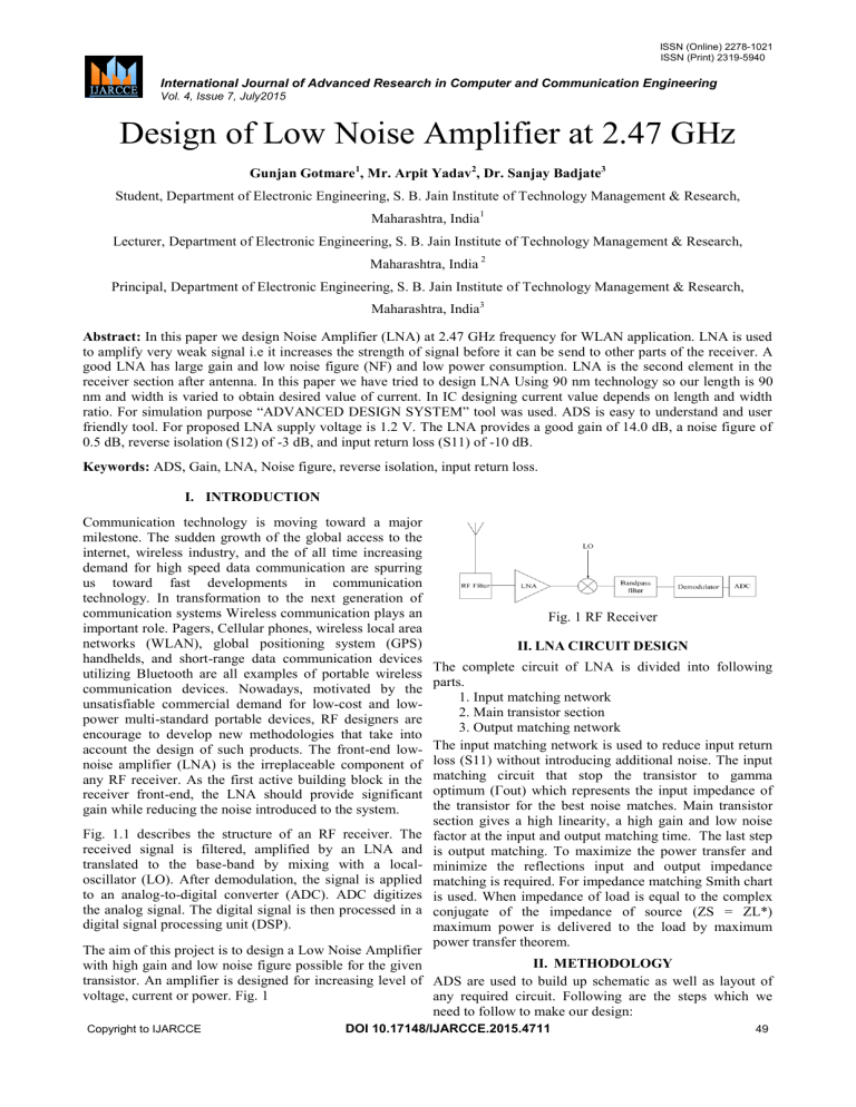
Fig. 1.1 describes the structure of an RF receiver. The received signal is filtered, amplified by an LNA and translated to the base-band by mixing with a localoscillator (LO). After demodulation, the signal is applied to an analog-to-digital converter (ADC). ADC digitizes the analog signal. The digital signal is then processed in a digital signal processing unit (DSP).
The aim of this project is to design a Low Noise Amplifier with high gain and low noise figure possible for the given transistor. An amplifier is designed for increasing level of voltage, current or power. Fig. 1 parts.
Fig. 1 RF Receiver
II.
LNA CIRCUIT DESIGN
The complete circuit of LNA is divided into following
1. Input matching network
2. Main transistor section
3. Output matching network
The input matching network is used to reduce input return loss (S11) without introducing additional noise. The input matching circuit that stop the transistor to gamma optimum (Γout) which represents the input impedance of the transistor for the best noise matches. Main transistor section gives a high linearity, a high gain and low noise factor at the input and output matching time. The last step is output matching. To maximize the power transfer and minimize the reflections input and output impedance matching is required. For impedance matching Smith chart is used. When impedance of load is equal to the complex conjugate of the impedance of source (ZS = ZL*) maximum power is delivered to the load by maximum power transfer theorem.
II.
METHODOLOGY
ADS are used to build up schematic as well as layout of any required circuit. Following are the steps which we need to follow to make our design:
Copyright to IJARCCE DOI 10.17148/IJARCCE.2015.4711 49
ISSN (Online) 2278-1021
ISSN (Print) 2319-5940
International Journal of Advanced Research in Computer and Communication Engineering
Vol. 4, Issue 7, July2015
A.
Creating a blank project
1 Start up ADS: Start > Programs > Advanced Design
System 2009 > Advanced Design System.
2 Open a new project and if the project has been already created, then open a project by double clicking on project name.
Open
Project
If the schematic window doesn’t open automatically then this button is use to open it.
3.
Make the schematic diagram as per requirement using circuit icons which can be select with the mouse cursor - just point and click. Hit escape to complete the selection of a particular part. We can select elements of the circuit from the Lumped Component of menu which includes
R, L, C, combinations of these, and ideal transformers.
The T-line menu consist of various types of transmission line circuit elements, ideal or modeled for the particular geometries of micro strip or other planar line configurations
B.
Selection of MOS Transistor
While designing an Low Noise Amplifier, selection of
MOS Transistor is the most important step. Due to mobility of electrons we have selected an enhancement type of n-MOS transistor. Drain to source voltage (V ds
), gate to source voltage (V gs
) and drain to source current
(I ds
) are the important parameters in the transistor. Values of V ds
and V gs
are predetermined. We have to calculate Ids value which is dependent on W/L ratio of MOS transistor.
Device length is fixed at 0.09 micrometer, since we are using 90 nm technologies. Ids depend on “width” of the device.
I ds
= (µ n*
C ox
/2)*(W/L ) *(V gs
-V t
)
2
Fig. 2 Selection of MOS schematic.
Fig. 3 Simulation Result
From above result:
I ds =
1.11mA
When V ds
= 1.8V & V gs
= 1.3V
V t
= 0.2 V
We know that
I ds
= (βn/2)*(W/L ) *(v gs
- V t
)
2 …………………...
(1)
After substituting above values in eq. (1)
βn = 179.03 μA/V …………………………(2)
C.
DC Simulation
Third step is DC simulation it is used to calculate the Q point i.e. quiescent point of the MOS device. DC
Simulation controller calculates the DC operating characteristics of a design which is under test (DUT). It checks topology and analyze the circuit’s power consumption and DC operating point. The simulator estimates the response of a circuit to a particular stimulus by formulating a system of circuit equations and then solving them mathematically.
DC simulation is set to sweep one or more parameters, enabling to perform tasks such as model parameters verification by comparing the simulated DC transfer characteristics (I-V curves) of the model with actual measurements. We can use following steps to perform DC
Simulation-
Palette window > Simulation DC > DC block > Parameter sweep (for V gs
& V ds
) > Variable.
Copyright to IJARCCE DOI 10.17148/IJARCCE.2015.4711 50
ISSN (Online) 2278-1021
ISSN (Print) 2319-5940
International Journal of Advanced Research in Computer and Communication Engineering
Vol. 4, Issue 7, July2015
Simulation Result:
Fig. 4 NMOS Circuit
Fig. 7 Common Source 2.47GHZ tuned LNA
Fig. 5 MOS Device I-V Characteristics
Above graph shows that the DC controller VGS sweeps from 0 to 0.9 V. First VDS =0, VGS is swept by 0.1V.
This continues until VDS=1.2 at which point the simulation is complete.
D.
S Parameter analysis
S11, S12, S21, S22 are referred to as the scattering parameters or the S-parameters. The parameters S11, S22 have the meaning of reflection coefficients, and S21, S12, the meaning of transmission coefficients. The input and output reflection in the circuits are calculated by S11 and forward and reverse voltage gain in dB are calculated by
S21 and S12 as shown in the figure 6
Fig. 6 S Parameter Two Port Model.
After DC biasing, feedback and blocking capacitor is added in network. This network is looks as follows
Fig. 8 Simulation Results
Fig. 9 Tuning Screen
III.
EXPECTED OUTCOME & FUTURE
We will design Low Noise Amplifier and will meet the following specification
1.
Frequency : 2.47GHz
2.
Gain :
3.
Noise Figure:0.5 dB
4.
Supply:
5.
Technology: 90nm
6.
S11: -10 dB
7.
Drain Current :1mA
14 dB
1.2 V
IV.
CONCLUSION
We have not achieved desired results of low noise amplifier. The improvement of this LNA is still going on
Copyright to IJARCCE DOI 10.17148/IJARCCE.2015.4711 51
ISSN (Online) 2278-1021
ISSN (Print) 2319-5940
International Journal of Advanced Research in Computer and Communication Engineering
Vol. 4, Issue 7, July2015 to achieve the desired results, we will modified the circuit and try to reduce its noise value as low as possible and gain as high as possible. We suppose to check the Sparameter, tuning parameter and harmonic balance.
ACKNOWLEDGMENT
The author thanks Dr. S. L. Badjate & Mr. Arpit Yadav from S. B.Jain Institute of Technology Management &
Research for technical discussion & processing support without whom this paper would never be completed.
REFERENCES
[1] T.T.N. Tran, C.C. Boon, M.A. Do and K.S. Yeo, Ultra-low power series input resonance differential common gate LNA,
ELECTRONICS LETTERS 9th June 2011 Vol. 47 No. 12.
[2] Thi Thu Nga Tran, Chim Chye Boon ,Manh Anh Do, and Kiat
Seng Yeo, A 2.4 GHz ultra low-power high gain LNA utilizing xmatch and capacitive feedback input network, 978-1-61284-857-
0/11/$26.00@2011 IEEE
[3] P. Andreani, H. Sjland, Noise Optimization of an Inductively
Degenerated CMOS Low Noise Amplifier, Analog and Digital
IEEE Trans. Circuit and Systems Signal Processing, vol.48, no. 9, pp. 835-841, Sep 2001.
[4] Member, IEE E, A Low-Power 2.4-GHz Receiver Front End With a
Lateral Current-Reusing Technique, IEEE TRANSACTIONS ON
CIRCUITS AND SYSTEMS—II: EXPRESS BRIEFS, VOL. 61,
NO. 8, AUGUST 2014
[5] Sumit Bagga, Andre L.Mansano, Wouter A. Serdijn, Fellow,John
R. Long Koen Van Hartingsveldtand Kathleen Philips, A
Frequency-Selective Broadband Low-Noise Amplifier With
Double-Loop Transformer Feedback, IEEE TRANSACTIONS ON
CIRCUITS AND SYSTEMS—I: REGULAR PAPERS, VOL. 61,
NO. 6, JUNE 2014
[6] C. W. Kim, M. S. Kang, P. T. Anh, H. T. Kim, S. G. Lee, An
Ultra-Wideband CMOS Low Noise Amplifier for 35GHz UWB
System, IEEE J. Solid-State Circuits, vol.40, no. 2, pp. 544-547,
Feb 2005.
[7] T. H. Lee, The Design of CMOS Radio-frequency Integrated
Circuits, 2nd ed., Cambridge, UK: Cambridge University Press
2004.
BIOGRAPHIES
Gunjan Gotmare, Student, M. Tech, S. B. Jain Institute of Technology Management & Research
Mr. Arpit Yadav M. Tech, G.H. Raisoni College of
Engineering, Nagpur Lecturer in S. B. Jain Institute of
Technology Management & Research
Dr.Sanjay Badjate Vice Principal in S. B. Jain Institute of Technology Management & Research
Copyright to IJARCCE DOI 10.17148/IJARCCE.2015.4711 52
